 ALLPCB


In the fast-evolving world of PCB design, via-in-pad technology has become a game-changer for engineers working on high-density interconnect (HDI) boards, especially when dealing with Ball Grid Array (BGA) components. If you're searching for ways to optimize space, enhance thermal performance, and improve signal integrity using via-in-pad filling techniques, you're in the right place. This blog dives deep into the essentials of via-in-pad (VIP) design, covering key aspects like filling methods, active pad PCB design, BGA routing with via-in-pad, planarization for via-in-pad, and the thermal performance of via-in-pad. Let's explore how to master this technique for your next project.
What is Via-in-Pad and Why Does It Matter?
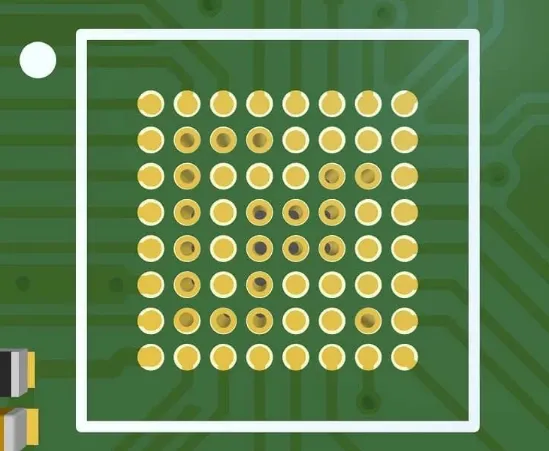
Via-in-pad is a PCB design technique where a via—a small hole that connects different layers of a circuit board—is placed directly inside a component pad, typically under a surface-mount device like a BGA. Unlike traditional vias placed outside pads, this method saves valuable board space and allows for tighter component layouts, making it ideal for compact, high-performance designs.
The importance of via-in-pad lies in its ability to support modern electronics' demand for miniaturization. As devices get smaller and more complex, engineers need solutions to fit more components into limited spaces without sacrificing performance. Via-in-pad addresses this by reducing routing complexity and improving electrical and thermal characteristics. However, to fully leverage its benefits, understanding via filling techniques is crucial. Let’s break down the details.
Understanding Via-in-Pad Filling Techniques
Via filling is a critical step in via-in-pad design to ensure reliability and performance. Without proper filling, vias can create issues like solder wicking (where solder flows into the via during assembly, causing poor connections) or uneven surfaces that affect component mounting. There are several via filling methods, each with specific applications based on design needs and manufacturing capabilities.
1. Conductive Via Filling
Conductive via filling uses materials like copper or silver paste to fill the via. This method enhances electrical conductivity and thermal dissipation, making it ideal for high-power applications. For instance, in a design with a BGA package handling high currents, conductive filling can reduce resistance in the via, ensuring stable performance. Typically, a conductivity value of around 0.017 micro-ohm-meter can be achieved with copper filling, significantly better than unfilled vias.
2. Non-Conductive Via Filling
Non-conductive filling involves using epoxy or resin to fill the via. This method focuses on mechanical stability and preventing solder wicking rather than improving electrical performance. It’s often used in designs where thermal and electrical demands are moderate but surface flatness is critical for soldering. Non-conductive fills are also generally more cost-effective than conductive options.
3. Via-in-Pad Plated Over (VIPPO)
VIPPO is a popular technique where the via is filled (often with epoxy) and then plated over with copper to create a flat, fully metalized surface. This ensures a smooth pad for component attachment and is widely used in HDI designs with fine-pitch BGAs. VIPPO requires a minimum copper plating thickness of around 5 micrometers for standard reliability (Class 2) and up to 12 micrometers for more demanding applications (Class 3).
Active Pad PCB Design with Via-in-Pad
Active pad PCB design refers to integrating vias directly into pads that are part of the active circuitry, such as under BGA components or other high-density packages. This approach maximizes space efficiency but comes with unique challenges. For instance, placing a via in an active pad requires precise alignment to avoid signal interference or manufacturing defects.
One key consideration in active pad design is ensuring the via doesn’t disrupt the solder joint. A poorly filled or misaligned via can create voids during soldering, leading to reliability issues. Using VIPPO or conductive filling helps create a uniform surface, reducing the risk of such problems. Additionally, active pads with vias must be designed with proper annular rings (the copper area surrounding the via) to maintain structural integrity. A typical annular ring width of 0.1 mm is recommended for most HDI boards.
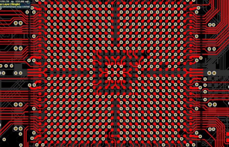
BGA Routing with Via-in-Pad
Routing for BGA components is notoriously challenging due to their high pin count and fine pitch (often as small as 0.4 mm). Via-in-pad technology is a lifesaver in these scenarios, as it allows vias to be placed directly under the BGA pads, freeing up space for routing on outer layers. This is especially useful in multilayer boards where signal traces need to escape from densely packed areas.
However, BGA routing with via-in-pad requires careful planning. For example, designers must ensure that the via size matches the pad dimensions to avoid manufacturing issues. A via diameter of 0.2 mm is often used for fine-pitch BGAs to balance drill precision and structural strength. Moreover, using conductive via filling can improve signal integrity by reducing impedance mismatches, which is critical for high-speed signals operating at frequencies above 1 GHz.
Planarization for Via-in-Pad: Achieving a Flat Surface
Planarization is the process of ensuring a flat surface over the via-in-pad area, which is essential for proper component mounting and soldering. Uneven surfaces can lead to inconsistent solder joints, especially in fine-pitch components where even a 0.05 mm height difference can cause failures.
In via-in-pad designs, planarization is typically achieved through the VIPPO technique, where the via is filled and plated over. This creates a seamless surface indistinguishable from a regular pad. During manufacturing, careful control of the plating process is necessary to avoid over-plating or under-plating, which can create bumps or dips. Some advanced processes use chemical mechanical polishing (CMP) to achieve surface flatness within 1-2 micrometers, ensuring optimal soldering results.
Planarization also impacts thermal performance, as a flat surface allows better contact between the component and the pad, facilitating heat transfer. For high-power BGAs, this can mean the difference between a reliable design and one prone to overheating.
Thermal Performance of Via-in-Pad
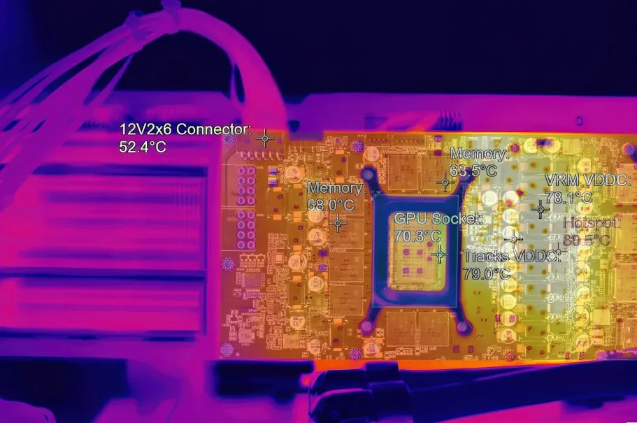
Thermal management is a critical factor in PCB design, especially for components like BGAs that generate significant heat. Via-in-pad technology can enhance thermal performance by providing a direct path for heat dissipation from the component to inner layers or heat sinks. Conductive via filling, particularly with copper, is highly effective in this regard due to its high thermal conductivity (approximately 400 W/m·K).
For example, in a design with a BGA dissipating 5 watts of heat, a via-in-pad with conductive filling can reduce the junction temperature by up to 10°C compared to an unfilled via, depending on the board stack-up. This improvement can extend the component's lifespan and prevent thermal throttling in high-performance applications.
However, thermal performance isn’t just about the via filling material. The number and placement of vias also matter. Using multiple vias under a single pad (often called a "via array") can further enhance heat dissipation. A common practice is to place 4-6 vias under larger pads to create multiple thermal paths, especially in designs with thick boards (over 2 mm).
Advantages and Challenges of Via-in-Pad Technology
Advantages
- Space Savings: By placing vias directly in pads, designers can reduce board size or fit more components into the same area.
- Improved Signal Integrity: Shorter signal paths and reduced inductance (often below 1 nH per via) enhance high-speed performance.
- Better Thermal Management: Direct heat paths through filled vias improve cooling efficiency.
Challenges
- Manufacturing Complexity: Via filling and planarization require precise processes, increasing production costs by 10-20% compared to traditional vias.
- Design Constraints: Vias in active pads must be carefully sized and placed to avoid signal or soldering issues.
- Reliability Risks: Improper filling can lead to voids or cracks, especially under thermal stress.
Best Practices for Implementing Via-in-Pad in Your Designs
To successfully incorporate via-in-pad technology, follow these practical tips:
- Choose the Right Filling Method: Use conductive filling for high-power or high-speed designs and non-conductive or VIPPO for cost-sensitive projects with moderate requirements.
- Optimize Via Size: Match via diameter to pad size, typically keeping it under 0.3 mm for fine-pitch components to ensure manufacturability.
- Ensure Proper Planarization: Work with your manufacturer to confirm surface flatness within 1-2 micrometers for reliable soldering.
- Simulate Thermal Performance: Use design software to model heat dissipation and place multiple vias where needed for thermal management.
- Test Prototypes: Validate your via-in-pad design with small-batch prototypes to identify potential issues before full-scale production.
Conclusion: Elevating PCB Design with Via-in-Pad Mastery
Via-in-pad technology, when paired with the right filling techniques, offers a powerful solution for modern PCB challenges like space constraints, signal integrity, and thermal management. Whether you're working on BGA routing with via-in-pad, focusing on active pad PCB design, or optimizing planarization for via-in-pad, understanding the nuances of this approach can significantly enhance your designs. By leveraging conductive or non-conductive fills and following best practices, you can achieve reliable, high-performance boards tailored to the demands of today’s electronics.
Mastering via-in-pad is not just about following trends—it’s about unlocking the full potential of your PCB layouts. With careful design and collaboration with manufacturing partners, you can push the boundaries of what’s possible in compact, high-density designs. Dive into via-in-pad techniques for your next project and see the difference in performance and efficiency.


