 ALLPCB


In the world of printed circuit board (PCB) manufacturing, ensuring quality and reliability is critical. One technology that has become a cornerstone of modern production is Automated Optical Inspection (AOI). So, is AOI needed? The answer is a resounding yes. AOI is essential for detecting defects, ensuring precision in PCB testing, and maintaining high standards in solder mask production. It saves time, reduces costs, and improves the overall quality of electronic products.
In this blog, we’ll dive deep into why AOI is indispensable in PCB manufacturing. We’ll explore its role in testing PCBs, its impact on solder mask testing, and trends in the solder mask production market. Whether you’re an engineer, a manufacturer, or simply curious about PCB technology, this guide will provide valuable insights into the importance of AOI.
What Is Automated Optical Inspection (AOI)?
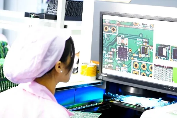
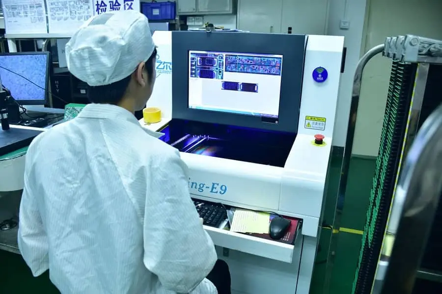
Automated Optical Inspection, or AOI, is a technology used to visually inspect PCBs for defects during the manufacturing process. Unlike manual inspection, which relies on human eyes and is prone to errors, AOI uses high-resolution cameras and advanced software to scan and analyze the board. It identifies issues such as missing components, solder defects, and misalignments with incredible accuracy.
AOI systems are typically integrated into various stages of PCB production, including bare board inspection, solder paste inspection, and post-reflow inspection. By automating the inspection process, manufacturers can achieve consistent results, even when dealing with complex designs or high-volume production.
Why Is AOI Needed in PCB Testing?
Testing PCBs is a critical step in ensuring that electronic devices function as intended. Without proper testing, defective boards can lead to product failures, costly recalls, or even safety hazards. Here’s why AOI is a game-changer in PCB testing:
- High Accuracy: AOI systems can detect defects as small as 0.01 mm, far beyond the capability of human inspectors. This precision is vital for modern PCBs, which often feature tiny components and intricate layouts.
- Speed: Manual inspection of a single PCB can take several minutes, while an AOI system can complete the same task in seconds. For high-volume production, this speed translates to significant time savings.
- Consistency: Human inspectors may miss defects due to fatigue or oversight, but AOI systems deliver consistent results, ensuring that every board meets the required standards.
- Cost-Effectiveness: While the initial investment in AOI equipment can be high, the reduction in labor costs and minimized rework expenses make it a cost-effective solution over time.
In PCB testing, AOI is often used after soldering to check for issues like solder bridges, insufficient solder, or misplaced components. By catching these problems early, manufacturers can avoid downstream issues that could compromise the final product.
The Role of AOI in Solder Mask Testing
Solder mask testing is a crucial aspect of PCB manufacturing. The solder mask is a protective layer applied to the board to prevent solder from bridging between conductive traces and to shield the board from environmental damage. Defects in the solder mask, such as pinholes, uneven coating, or misalignment, can lead to short circuits or corrosion over time.
AOI plays a vital role in solder mask testing by providing a non-contact method to inspect the quality of the mask. Here’s how AOI contributes:
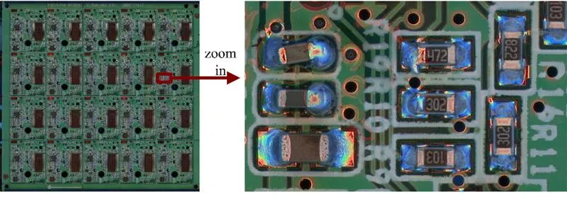
- Detecting Surface Defects: AOI systems can identify surface irregularities in the solder mask, such as bubbles or cracks, which could expose the underlying copper traces.
- Ensuring Alignment: The solder mask must align perfectly with the PCB’s design to cover the correct areas. AOI verifies this alignment with precision, ensuring that no conductive areas are left exposed.
- Identifying Color and Finish Issues: Solder masks come in various finishes, such as matte or glossy. A glossy finish, for instance, can sometimes cause glare during inspection, leading to false positives. Advanced AOI systems can be calibrated to account for these variations, ensuring accurate results.
By integrating AOI into solder mask testing, manufacturers can ensure that the protective layer performs its role effectively, ultimately enhancing the durability and reliability of the PCB.
AOI and the Solder Mask Production Market
The solder mask production market has seen significant growth in recent years, driven by the increasing demand for high-quality PCBs in industries like consumer electronics, automotive, and telecommunications. As PCBs become more complex, the need for precise solder mask application and inspection has never been greater.
According to recent industry reports, the global market for automated inspection systems, including AOI, is projected to grow at a compound annual growth rate (CAGR) of over 13% from 2023 to 2030, reaching a value of approximately USD 72.9 billion by the end of the decade. This growth is closely tied to advancements in PCB manufacturing and the rising adoption of automation technologies.
In the context of the solder mask production market, AOI systems are becoming indispensable for several reasons:
- Increasing Complexity: Modern PCBs often feature high-density interconnects (HDI) with trace widths as small as 0.075 mm. Applying and inspecting solder masks on such designs requires the precision that only AOI can provide.
- Quality Standards: Industries like automotive and aerospace have stringent quality requirements. AOI ensures that solder masks meet these standards by detecting even the smallest defects.
- Environmental Considerations: Solder masks must withstand harsh environmental conditions, such as humidity and temperature fluctuations. AOI helps verify that the mask is applied uniformly to provide adequate protection.
As the solder mask production market continues to evolve, manufacturers are increasingly relying on AOI to maintain a competitive edge. The technology not only improves product quality but also streamlines production processes, reducing waste and enhancing efficiency.
Benefits of AOI Beyond Defect Detection
While AOI is primarily known for its role in defect detection, its benefits extend far beyond that. Here are some additional advantages that make AOI a must-have in PCB manufacturing:
- Data Collection and Analysis: AOI systems generate detailed reports on defects and production trends. This data can be used to identify recurring issues, optimize processes, and improve overall yield rates. For instance, if a specific soldering defect occurs frequently, manufacturers can adjust their equipment settings to prevent future occurrences.
- Integration with Other Systems: AOI can be integrated with other inspection technologies, such as X-ray inspection, to provide a comprehensive quality control solution. This is especially useful for multilayer PCBs, where internal defects may not be visible to optical systems alone.
- Scalability: AOI systems are adaptable to different production volumes. Whether you’re producing a small batch of prototypes or millions of units for mass production, AOI can scale to meet your needs without compromising accuracy.
These benefits highlight why AOI is not just a tool for inspection but a strategic asset for manufacturers looking to stay ahead in a competitive industry.
Challenges of Implementing AOI and How to Overcome Them
Despite its many advantages, implementing AOI in PCB manufacturing is not without challenges. Understanding these hurdles and how to address them can help manufacturers make the most of this technology.
- High Initial Cost: AOI systems can be expensive to purchase and install. However, the long-term savings in labor costs and reduced rework often outweigh the upfront investment. Manufacturers can also explore leasing options or start with smaller-scale systems before scaling up.
- Programming Complexity: Setting up an AOI system requires programming to match the specific design of each PCB. This can be time-consuming, especially for custom designs. Working with experienced technicians or investing in user-friendly software can simplify this process.
- False Positives: In some cases, AOI systems may flag non-defects as issues, especially when dealing with reflective surfaces like glossy solder masks. Regular calibration and software updates can minimize false positives, ensuring accurate inspections.
By addressing these challenges, manufacturers can fully harness the power of AOI to improve their production processes.
How AOI Enhances Overall Manufacturing Efficiency
In addition to improving quality, AOI significantly enhances manufacturing efficiency. By automating the inspection process, it reduces the need for manual labor, which is often a bottleneck in production lines. This allows manufacturers to allocate human resources to other critical tasks, such as design optimization or customer support.
Moreover, AOI minimizes the risk of defective products reaching the market. For example, catching a solder bridge defect during the post-reflow stage prevents the need for costly repairs or replacements later in the supply chain. This not only saves money but also protects the manufacturer’s reputation for reliability.
Finally, AOI supports faster time-to-market. With quicker inspections and fewer delays caused by defects, manufacturers can meet tight deadlines without compromising on quality. In industries where speed is a competitive advantage, this can make a significant difference.
Future Trends: AOI and the Evolution of PCB Manufacturing
As technology continues to advance, AOI systems are evolving to meet the demands of next-generation PCB manufacturing. Here are some trends to watch:
- 3D AOI: Traditional 2D AOI systems are being supplemented by 3D systems that can measure height and depth, providing even greater accuracy in detecting defects like lifted components or uneven solder joints.
- Artificial Intelligence (AI): AI-powered AOI systems are becoming more common, enabling machines to learn from past inspections and improve their defect detection capabilities over time.
- Integration with Industry 4.0: AOI is increasingly being integrated into smart manufacturing environments, where data from multiple systems is shared in real-time to optimize production processes.
These advancements suggest that AOI will remain a critical component of PCB manufacturing for years to come, adapting to the growing complexity of electronic devices.
Conclusion: The Indispensable Role of AOI
Automated Optical Inspection (AOI) is not just a luxury but a necessity in modern PCB manufacturing. From ensuring precision in PCB testing to enhancing solder mask quality and meeting the demands of the solder mask production market, AOI delivers unmatched accuracy, speed, and efficiency. Its ability to detect defects, reduce costs, and improve overall product reliability makes it an essential tool for manufacturers aiming to stay competitive.
By integrating AOI into their production lines, manufacturers can achieve higher quality standards, streamline operations, and adapt to the evolving needs of the electronics industry. As technology continues to advance, AOI will only become more integral to the future of PCB manufacturing.


