ALLPCB


If you're looking to understand PCB copper balance DFM, figure out what is distribution for DFM, or learn balancing PCB DFM, you're in the right place. Copper distribution in PCB design is a critical factor for ensuring manufacturability, performance, and reliability. With the help of Design for Manufacturability (DFM) software, you can achieve balanced copper distribution to avoid issues like warping, uneven etching, or thermal imbalances. In this guide, we'll break down the importance of copper distribution, how DFM tools assist in balancing it, and practical tips to optimize your PCB designs.
This comprehensive blog will walk you through the essentials of copper distribution, the role of DFM software, and actionable strategies to ensure your PCB designs are ready for efficient manufacturing. Let’s dive in!
What is Distribution for DFM in PCB Design?
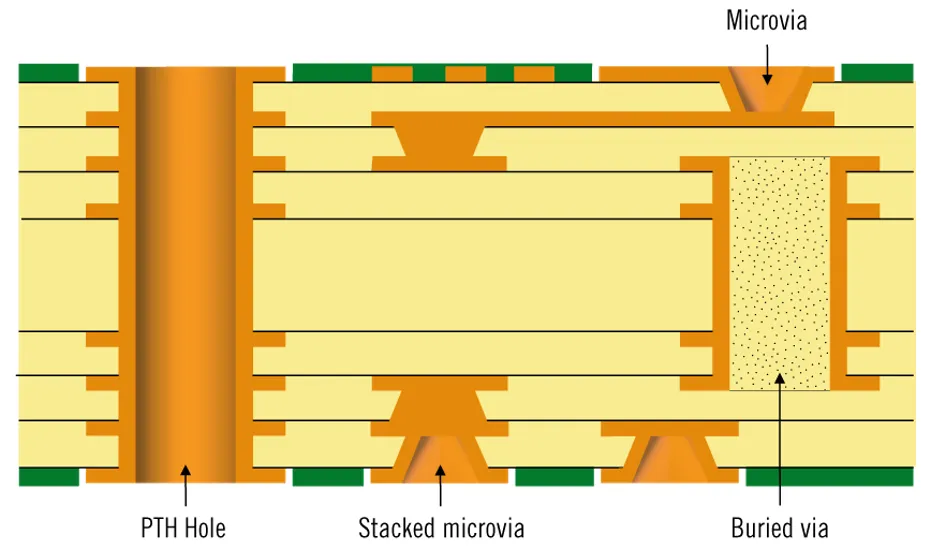
In the context of PCB design, distribution for DFM refers to the strategic placement and balancing of materials—especially copper—across the board to ensure it can be manufactured without defects or performance issues. Copper distribution specifically focuses on evenly spreading copper traces, planes, and features on each layer of the PCB. Uneven copper distribution can lead to problems like board warping during soldering, inconsistent etching during fabrication, and thermal hotspots that affect component performance.
Design for Manufacturability (DFM) is a set of guidelines and practices that optimize a PCB design for efficient production. When it comes to copper, DFM ensures that the amount and placement of copper are balanced to meet manufacturing tolerances and prevent issues. For example, if one side of a PCB layer has significantly more copper than the other, it can cause stress during the lamination process, leading to a warped board. DFM software helps identify and correct these imbalances early in the design phase.
Why PCB Copper Balance Matters in DFM
Achieving PCB copper balance DFM is essential for several reasons. Copper imbalance can directly impact the structural integrity, thermal management, and electrical performance of a PCB. Here are some key reasons why copper balance is critical:
- Preventing Warpage: During the manufacturing process, uneven copper distribution can cause the PCB to bend or warp due to differences in thermal expansion. A balanced design minimizes stress and keeps the board flat.
- Ensuring Uniform Etching: In the etching process, areas with dense copper may etch slower than areas with less copper, leading to inconsistent trace widths or potential defects. Balanced copper distribution ensures uniform etching results.
- Thermal Management: Copper conducts heat, so uneven distribution can create hotspots on the board, affecting component reliability. Balanced copper helps distribute heat evenly.
- Signal Integrity: For high-speed designs, copper balance impacts impedance control. Uneven copper can lead to variations in impedance (e.g., deviating from a target of 50 ohms), causing signal reflection and data loss.
How DFM Software Helps with Copper Distribution
DFM software plays a vital role in helping designers achieve PCB copper balance DFM. These tools analyze your PCB layout and provide feedback on potential manufacturing issues, including copper distribution problems. Here’s how DFM software supports balanced copper design:
- Automated Copper Balance Checks: DFM tools scan each layer of your PCB to measure copper density. If one area has significantly more copper (e.g., a density of 80% on one side versus 20% on the other), the software flags it as a potential issue.
- Copper Thieving and Hatching: Many DFM tools suggest or automatically add copper thieving (small, non-functional copper dots) or hatching patterns to balance out low-density areas. This ensures uniform copper coverage without affecting the circuit’s functionality.
- Thermal Analysis: Advanced DFM software simulates heat dissipation across the board, identifying areas where uneven copper might cause thermal imbalances. This is crucial for high-power designs where heat management is critical.
- Manufacturing Rule Compliance: DFM software enforces manufacturing constraints, such as minimum copper spacing (e.g., 3 mils for traces) and clearance rules, to ensure the design is feasible for production.
By integrating DFM software into your workflow, you can catch copper distribution issues before sending the design to fabrication, saving time and reducing costs associated with redesigns or defective boards.
Key Techniques to Learn Balancing PCB DFM
If you want to learn balancing PCB DFM, there are several practical techniques you can apply during the design phase. These methods, often supported by DFM software, ensure that copper distribution is optimized for manufacturing. Let’s explore them in detail:
1. Use Copper Thieving for Balance
Copper thieving involves adding small, non-functional copper shapes or dots in areas with low copper density. This technique balances the overall copper coverage on a layer, reducing the risk of uneven etching or warpage. For example, if a layer has a large ground plane on one side (80% copper) and minimal traces on the other (20% copper), adding thieving dots can bring the density closer to 50% on both sides.
2. Implement Hatching Patterns
Hatching is another method to balance copper by filling empty spaces with a grid or crosshatch pattern of copper. This is particularly useful for large ground or power planes. Hatching reduces the amount of solid copper while maintaining electrical connectivity and balancing density. DFM tools often recommend a hatching density (e.g., 50% fill) based on manufacturing requirements.
3. Mirror Copper on Double-Sided Boards
For double-sided PCBs, ensure that copper distribution is mirrored or balanced between the top and bottom layers. If the top layer has a dense copper area, try to replicate a similar density on the bottom layer. This symmetry reduces mechanical stress during manufacturing, preventing warpage.
4. Avoid Large Copper-Free Areas
Large areas without copper can cause uneven stress during lamination and soldering. If such areas are unavoidable due to design constraints, use copper thieving or hatching to fill them. For instance, if a 2-inch by 2-inch section of your board has no traces, adding a hatched copper pattern can prevent manufacturing issues.
5. Check Copper Weight and Thickness
Copper weight, measured in ounces per square foot (oz/ft2), affects thermal and electrical performance. Standard copper weights are 1 oz/ft2 (35 microns thick) and 2 oz/ft2 (70 microns thick). Ensure that the copper weight is consistent across layers unless specific design needs (e.g., high-current paths) require heavier copper. DFM software can flag mismatches in copper weight that might affect balance.
Common Copper Distribution Issues and How to Fix Them
Even with the best intentions, copper distribution issues can arise in PCB design. Here are some common problems and how DFM software and best practices can help resolve them:
- Uneven Copper Density: This often happens when large ground planes are placed on one side of a layer while the other side has minimal traces. Use DFM software to identify density differences and apply copper thieving or hatching to balance it out.
- Thermal Hotspots: High-power components or dense copper areas can create hotspots. DFM tools with thermal simulation can pinpoint these areas, allowing you to redistribute copper or add thermal vias (e.g., 10-mil diameter vias spaced 50 mils apart) for heat dissipation.
- Impedance Mismatch: For high-speed signals, uneven copper near traces can alter impedance. If a design targets 50-ohm impedance, variations due to copper imbalance can cause signal issues. Use DFM software to check trace surroundings and adjust copper placement.
Benefits of Balanced Copper Distribution with DFM
Investing time in achieving PCB copper balance DFM offers several long-term benefits for your designs and manufacturing process. Here are some advantages:
- Improved Manufacturing Yield: Balanced copper reduces the likelihood of defects during fabrication, leading to higher yield rates and fewer rejected boards.
- Cost Savings: By catching issues early with DFM software, you avoid costly redesigns and manufacturing delays. For instance, fixing a copper imbalance in the design phase is far cheaper than scrapping a batch of warped boards.
- Enhanced Reliability: Balanced copper ensures consistent thermal and electrical performance, increasing the lifespan and reliability of your PCB in real-world applications.
- Faster Time to Market: A design optimized for manufacturability moves through production smoothly, reducing lead times and getting your product to market faster.
Practical Tips for Using DFM Software for Copper Balance
To make the most of DFM software and ensure optimal copper distribution, follow these practical tips during your design process:
- Run DFM Checks Early: Don’t wait until the final design stage to run DFM analysis. Check copper balance after completing each layer to catch issues early.
- Customize DFM Rules: Tailor the DFM rules in your software to match your manufacturer’s specific requirements, such as minimum copper density or spacing (e.g., 4-mil clearance for high-density designs).
- Simulate Before Finalizing: Use the simulation features in DFM tools to test thermal and mechanical stress caused by copper distribution. Adjust the design based on the results.
- Collaborate with Manufacturers: Share DFM reports with your manufacturing partner to confirm that the copper balance meets their capabilities and standards.
Conclusion
Mastering PCB copper balance DFM is a game-changer for creating reliable, high-quality printed circuit boards. Understanding what is distribution for DFM and taking steps to learn balancing PCB DFM can significantly improve your design’s manufacturability and performance. With the help of DFM software, you can automate copper balance checks, apply techniques like thieving and hatching, and avoid common pitfalls that lead to manufacturing defects.
By following the guidelines and techniques outlined in this guide, you’ll be well-equipped to optimize copper distribution in your PCB designs. Balanced copper not only ensures smoother fabrication but also enhances the thermal, electrical, and mechanical stability of your boards. Start integrating DFM practices into your workflow today, and see the difference it makes in your next project!