Are you looking for ways to improve your PCB design without breaking the bank? Optimizing your PCB ground plane with budget-friendly copper pour techniques is a smart solution. In this guide, we’ll explore cheap PCB grounding methods, budget copper pour strategies, and DIY ground plane tips to help you achieve better signal integrity and reduce noise. Whether you’re a hobbyist or a professional engineer, these copper pour hacks will show you how to get the most out of your design while keeping costs low.
Let’s dive into the details of optimizing PCB ground planes with practical, actionable steps you can apply to your next project. From understanding the basics of ground planes to implementing cost-effective tricks, this blog covers everything you need to know.
What Is a PCB Ground Plane and Why Does It Matter?
A ground plane in a printed circuit board (PCB) is a large area of copper connected to the ground signal of your circuit. It serves as a return path for current, helps reduce electromagnetic interference (EMI), and stabilizes voltage levels. A well-designed ground plane can significantly improve signal integrity, especially in high-speed or high-frequency designs.
Without a proper ground plane, your PCB might suffer from issues like noise, crosstalk, or unstable power delivery. For budget-conscious designers, using copper pour to create an effective ground plane is one of the most affordable ways to enhance performance. The good news? You don’t need expensive tools or materials to make it work.
Benefits of Optimizing Your PCB Ground Plane
Before we get into the hacks, let’s look at why optimizing PCB ground planes is worth your time, especially on a budget:
- Noise Reduction: A solid ground plane minimizes ground loops and reduces noise in your circuit, which is critical for analog and mixed-signal designs.
- Improved Signal Integrity: Consistent grounding prevents signal distortion, especially in high-speed designs where signals can reach speeds of 1 GHz or more.
- Better Power Distribution: A ground plane paired with a power plane ensures stable voltage delivery, reducing drops that can affect performance.
- Cost-Effective EMI Control: Ground planes help shield your circuit from external interference without the need for additional components.
With these benefits in mind, let’s explore how to achieve them using cheap PCB grounding techniques and budget copper pour methods.
Copper Pour Basics: Getting Started on a Budget
Copper pour refers to filling unused areas of your PCB with copper, often connected to ground or power nets. It’s a simple yet powerful way to create a ground plane without adding extra layers or costs to your design. Here’s how to start with a DIY ground plane using copper pour:
- Use Free or Low-Cost Design Software: Many design tools offer free versions with copper pour features. These tools let you define areas for ground planes easily.
- Maximize Unused Space: Fill empty spaces on your PCB layout with copper connected to ground. This increases the ground plane area without additional material costs.
- Single-Layer Boards: If you’re working on a single-layer PCB to save money, use copper pour on one side for grounding while routing signals on the other. This keeps fabrication costs as low as $5–$10 for small batches.
Top 5 Copper Pour Hacks for Optimizing PCB Ground on a Budget
Now, let’s get into specific copper pour hacks that can take your ground plane design to the next level without increasing costs. These tips are tailored for engineers looking for cheap PCB grounding solutions and effective budget copper pour strategies.
1. Split Your Ground Plane for Mixed-Signal Designs
In mixed-signal PCBs with both analog and digital components, a single ground plane can lead to noise coupling. Instead, split your ground plane into separate analog and digital sections, connected at a single point (often near the power supply). This prevents digital noise from interfering with sensitive analog signals, maintaining signal integrity for frequencies as low as 100 kHz.
How to Do It on a Budget: Use your design software to define two copper pour regions and connect them with a narrow trace or a single via. This costs nothing extra and works well even on two-layer boards.
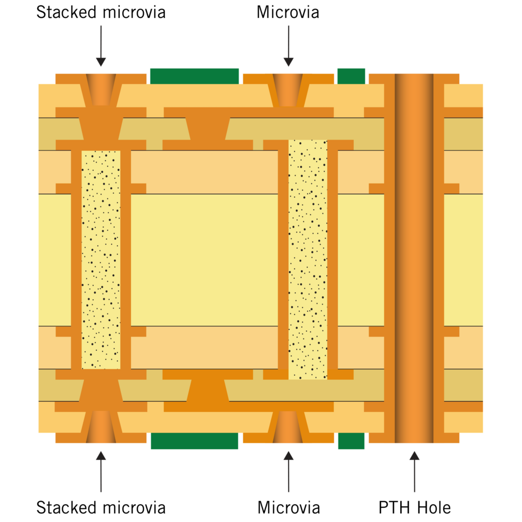
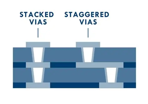
2. Add Ground Vias for Multi-Layer Boards
If your budget allows for a multi-layer PCB (often starting at $15 for small prototypes), use ground vias to connect ground planes across layers. This creates a low-impedance path (typically below 1 mΩ per via) for return currents, reducing noise and improving performance in high-speed designs.
Budget Tip: Place vias strategically near high-current components instead of scattering them everywhere. This minimizes drilling costs during fabrication while still achieving effective grounding.
3. Avoid Dead Copper with Thermal Reliefs
Dead copper refers to isolated copper areas that aren’t connected to any net. These can act as antennas, picking up noise and causing EMI issues. When using copper pour, ensure all areas are connected to ground or remove unconnected copper during the design phase.
Budget Hack: Use thermal reliefs (small gaps in copper around pads) to prevent heat dissipation issues during soldering. Most design tools let you set this up for free, ensuring your DIY ground plane doesn’t cause manufacturing problems.
4. Optimize Ground Plane Coverage with Grid Patterns
If a solid copper pour increases fabrication costs due to material usage, consider using a grid or hatched pattern for your ground plane. A grid with 50% copper coverage can still provide effective grounding while reducing copper usage, cutting costs by up to 10–20% on larger boards.
How to Implement: In your design software, set the copper pour to a hatched pattern with a spacing of 0.5–1 mm. This maintains a low-impedance path (around 5–10 mΩ) for return currents while saving on material.
5. Minimize Ground Loops with Short Return Paths
Ground loops occur when return currents take long, winding paths, creating noise and interference. To avoid this, place components close to their ground connections and keep return paths short. For example, in a 5V digital circuit, a ground loop longer than 10 cm can introduce noise levels above 50 mV.
Budget Solution: Rearrange your layout to group components by function (e.g., power, signal, control) and pour copper directly beneath them. This costs nothing and significantly improves performance.
Common Mistakes to Avoid in Budget Ground Plane Design
While working on cheap PCB grounding and budget copper pour designs, it’s easy to make mistakes that hurt performance. Here are some pitfalls to watch out for:
- Overlapping Ground and Power Planes: Without proper separation, this can cause capacitance issues, leading to noise. Keep at least 0.5 mm spacing between planes.
- Ignoring High-Speed Signals: High-speed traces (above 50 MHz) need a continuous ground plane underneath to avoid impedance mismatches (target 50 Ω for most designs).
- Skipping Design Rule Checks (DRC): Always run a DRC in your software to catch unconnected copper or spacing errors before fabrication.
Tools and Resources for DIY Ground Plane Design
Creating a DIY ground plane doesn’t require expensive tools. Here are some accessible resources to help you with optimizing PCB ground designs:
- Free Design Software: Tools like KiCad or Fritzing offer copper pour features and are perfect for budget designs.
- Online Calculators: Use free impedance calculators to determine optimal trace widths and ground plane spacing for your design.
- Community Forums: Engage with online communities for tips on copper pour hacks and low-cost PCB strategies.
Conclusion: Build Better PCBs Without Breaking the Bank
Optimizing your PCB ground plane doesn’t have to be expensive. With these copper pour hacks, you can achieve professional-grade grounding using cheap PCB grounding techniques and budget copper pour strategies. From splitting ground planes for mixed-signal designs to using grid patterns for cost savings, these DIY ground plane tips are practical and effective for any engineer.
By focusing on optimizing PCB ground design, you’ll improve signal integrity, reduce noise, and save money—all without compromising on quality. Start applying these methods to your next project and see the difference a well-designed ground plane can make.
 ALLPCB


