If you're looking to cut down on PCB manufacturing costs without compromising quality, following Design for Manufacturability (DFM) rules is the key. These guidelines help streamline the production process, reduce errors, and save money by optimizing your design for efficient fabrication and assembly. In this comprehensive guide, we’ll dive into essential PCB DFM rules focusing on cost reduction through strategies like optimizing layer count, choosing the right via types, setting appropriate trace widths, selecting cost-effective materials, improving panelization, and minimizing holes.
Whether you're an experienced engineer or new to PCB design, these practical tips will help you create designs that are both high-performing and budget-friendly. Let’s explore how to apply these DFM principles to your next project.
What Are PCB DFM Rules and Why Do They Matter for Cost Reduction?
PCB DFM rules are a set of design guidelines that ensure your printed circuit board is easy to manufacture. By following these rules, you can avoid common design mistakes that lead to production delays, reworks, or added expenses. DFM focuses on aligning your design with the capabilities of manufacturing processes, which directly impacts the overall cost.
Manufacturing costs can spiral out of control due to complex designs, unnecessary features, or overlooked details. For instance, adding extra layers or using specialized materials without justification can drive up expenses. By applying DFM principles, you minimize these risks and create a design that’s efficient to produce, saving both time and money.
Key PCB DFM Rules for Cost Reduction
Below, we break down the most critical DFM rules that target cost savings. Each section focuses on a specific aspect of PCB design, from layer count to hole minimization, with actionable advice you can implement right away.
1. Optimize Layer Count for Cost Efficiency
The number of layers in your PCB has a significant impact on manufacturing costs. Each additional layer increases the complexity of fabrication, requiring more materials and processing time. As a general rule, keep the layer count as low as possible while still meeting your design requirements.
For many applications, a 2-layer board is sufficient for simple circuits with low-speed signals. If your design involves high-speed signals or complex routing, you might need 4 or 6 layers, but always evaluate if the added layers are necessary. For example, a 4-layer board might cost 30-50% more than a 2-layer board due to additional lamination and drilling steps. Avoid jumping to higher layer counts unless impedance control (typically around 50 ohms for standard applications) or signal integrity demands it.
Tip: Use design software to simulate signal performance and routing density before adding layers. This can help confirm whether a simpler stack-up will work.
2. Choose the Right Via Types to Reduce Fabrication Costs
Vias are essential for connecting different layers of a PCB, but not all via types are created equal when it comes to cost. There are three main types to consider: through-hole vias, blind vias, and buried vias. Each has its place, but using the simplest option can save money.
- Through-Hole Vias: These are the most cost-effective as they go through all layers of the board and are easier to drill. Use these whenever possible.
- Blind Vias: These connect an outer layer to an inner layer without going through the entire board. They are more expensive due to additional manufacturing steps like sequential lamination.
- Buried Vias: These connect inner layers only and are the most costly because they require precise drilling and alignment during production.
For cost reduction, stick to through-hole vias unless your design specifically requires blind or buried vias for high-density interconnects or space constraints. For instance, using blind vias can increase costs by 20-30% compared to standard through-hole vias.
Tip: Minimize the total number of vias by optimizing trace routing. Fewer vias mean less drilling, which reduces both time and cost.
3. Set Appropriate Trace Width and Spacing for Manufacturability
Trace width and spacing directly affect how easily a PCB can be manufactured. If traces are too narrow or spaced too closely, manufacturers may need specialized equipment or additional process controls, which drive up costs. Standard trace widths and spacing are typically more cost-effective because they align with common fabrication capabilities.
For most designs, a trace width of 6-8 mils (0.006-0.008 inches) and spacing of 6 mils are achievable with standard processes. If you go below 4 mils, you may enter the realm of micro-fabrication, which can increase costs by 25% or more due to the need for finer etching and inspection tools. Always check the minimum trace width and spacing supported by your fabrication house to avoid unnecessary expenses.
Additionally, consider current-carrying capacity when setting trace widths. For a 1-ounce copper layer, a 10-mil trace can safely carry about 1 amp of current at room temperature. Oversizing traces beyond what’s needed wastes board space and material, while undersizing can lead to overheating or signal issues.
4. Select Cost-Effective Materials Without Sacrificing Performance
Material selection is another area where DFM rules can significantly impact costs. The substrate material, copper weight, and surface finish all play a role in the final price of your PCB.
- Substrate Material: FR-4 is the most common and cost-effective material for standard PCBs, suitable for frequencies up to about 1 GHz. For high-frequency designs (above 1 GHz), you might need materials like Rogers or Isola, but these can cost 2-3 times more than FR-4. Only use specialized materials if your design demands it.
- Copper Weight: Standard 1-ounce copper is sufficient for most low-power applications. Heavier copper (2 or 3 ounces) is more expensive and harder to etch, so reserve it for high-current designs.
- Surface Finish: HASL (Hot Air Solder Leveling) is the least expensive surface finish and works well for many applications. ENIG (Electroless Nickel Immersion Gold) offers better corrosion resistance but can cost 10-20% more. Choose based on your project’s needs, not just aesthetics.
Tip: Discuss material options with your manufacturer early in the design phase to balance cost and performance requirements.
5. Improve Panelization for Efficient Production
Panelization refers to how multiple PCBs are arranged on a single panel during manufacturing. Efficient panelization can reduce material waste and lower production costs. If your design is small, fitting multiple boards onto one panel maximizes the use of raw materials and minimizes per-unit costs.
Work with your manufacturer to understand their panel size constraints, typically around 18 x 24 inches for standard processes. Leave adequate spacing (about 0.1 inches) between boards for cutting or depanelization. Avoid irregular shapes or overly tight spacing, as these can complicate the process and increase costs due to potential breakage or tooling issues.
Also, consider using V-scoring or mouse bites for depanelization instead of routing, as these methods are often cheaper and faster for straight-edged designs. Efficient panelization can reduce costs by up to 15% by optimizing material usage.
6. Minimize Holes to Simplify Drilling and Reduce Costs
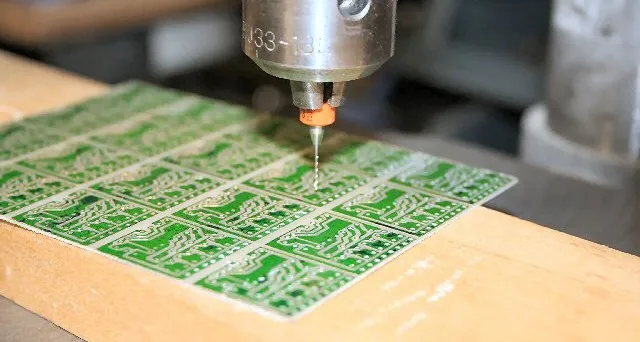
Every hole in a PCB, whether for vias, mounting, or components, requires drilling, which adds to manufacturing time and cost. Reducing the number of holes and standardizing their sizes can lead to significant savings.
For instance, limit the variety of drill sizes in your design. Using a single drill size for all holes (where possible) allows manufacturers to complete drilling in one pass, avoiding tool changes that slow down production. Each additional drill size can add 5-10% to the cost due to setup time. A common drill size for through-hole components is 0.035 inches, which works for many standard parts.
Additionally, avoid non-essential mounting holes or overly complex cutouts unless they are critical to the design. Fewer holes mean less drilling time and lower risk of defects during fabrication.
Tip: Review your component choices to favor surface-mount devices (SMDs) over through-hole components when possible, as SMDs don’t require drilled holes for leads.
Additional DFM Tips for Cost-Effective PCB Design
Beyond the core areas above, here are a few more DFM practices to keep costs in check:
- Standardize Component Sizes: Use common component packages (like 0805 or 0603 for resistors and capacitors) to avoid sourcing issues or assembly complications.
- Avoid Tight Tolerances: Unless your design requires precision (e.g., for high-speed signals at 10 GHz), stick to standard tolerances for dimensions and placements to simplify manufacturing.
- Design for Automation: Ensure your layout supports automated assembly processes by placing components on one side of the board if possible. Dual-sided assembly can increase costs by 20-30%.
Benefits of Following PCB DFM Rules for Cost Reduction
Adhering to DFM guidelines offers several advantages beyond just saving money:
- Faster Turnaround Times: Simplified designs are quicker to fabricate and assemble, reducing lead times.
- Higher Yield Rates: Fewer design errors mean less rework and higher production yields, saving on scrap costs.
- Improved Reliability: DFM-optimized designs are less prone to manufacturing defects, leading to more reliable products.
For example, a well-optimized design with minimal layers and standard materials can cut production costs by up to 40% compared to a complex, non-DFM-compliant design, while still meeting performance goals.
Partner with Experts for DFM Success
Designing a cost-effective PCB doesn’t have to be a solo endeavor. Collaborating with experienced manufacturing partners can provide valuable insights into DFM practices tailored to your project. At ALLPCB, we offer comprehensive support to help you refine your designs for maximum efficiency and affordability. From layer optimization to material selection, our team is ready to guide you through every step of the process.
Conclusion: Start Saving with PCB DFM Rules Today
Minimizing manufacturing costs for your PCB doesn’t mean cutting corners on quality. By following essential DFM rules—optimizing layer count, selecting the right via types, setting practical trace widths, choosing cost-effective materials, improving panelization, and minimizing holes—you can achieve significant savings while maintaining performance. Start implementing these guidelines in your next design to streamline production and keep your budget in check.
With a focus on practical, actionable strategies, you’re now equipped to tackle cost reduction head-on. Apply these PCB DFM rules to your projects and watch as efficiency and savings go hand in hand.
 ALLPCB


