ALLPCB


Overview
Circuit protection techniques and PCB layout strategies help improve safety, reliability, and connectivity. Wearable devices face a unique challenge compared with many IoT endpoints: the human body generates static charge during movement. Electrostatic discharge (ESD) can damage the sensitive electronics that support IoT applications.
Human Body Model and ESD Testing
To understand ESD susceptibility, start with the human body model (HBM), which is used to describe an integrated circuit's sensitivity to electrostatic discharge. A common HBM test model is defined in military standard MIL-STD-883, method 3015.8, and a similar international standard is JEDEC JS-001. Both models simulate a charged person with a 100 pF capacitor and a 1.5 kΩ discharge resistor. In testing, the capacitor is charged from about 250 V up to 8 kV and then discharged through the 1.5 kΩ resistor into the device under test.
ESD Risks Specific to Wearables
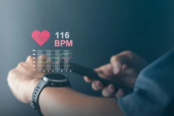
Because wearable devices are designed for close contact with the human body, they are continually exposed to static events generated by user interaction. Without proper protection, sensor circuits, battery charging interfaces, buttons, or data I/O ports on wearables can be damaged by ESD levels similar to those produced in HBM testing. Failure of a wearable device can impact the functionality and reliability of a broader system.
Design Recommendations
Applying advanced circuit protection techniques and careful PCB layout early in the design process helps improve performance, safety, and reliability of wearable designs. The following recommendations address common constraints in wearable electronics.
1. Small packages can still provide strong ESD protection
A key design challenge is the shrinking size of wearable devices. Historically, large-structure diodes required large packages. Designers should prefer unidirectional diode configurations when possible, since they tend to perform better during negative-polarity ESD events. During a negative ESD event, the clamp voltage of a unidirectional diode is based on the diode's forward bias (typically under 1.0 V). By contrast, a bidirectional diode clamps based on reverse breakdown voltage during negative events, which is higher than the forward bias of a unidirectional diode. Therefore, a unidirectional configuration can significantly reduce stress on the system during negative ESD transients.
2. Place diodes judiciously
Not every IC pin in a wearable requires a board-level TVS diode. Identify pins that are exposed to potential user contact or external ESD sources. Interfaces that can be touched by a user, such as USB ports, buttons/switches, and data buses, are common entry points for ESD. Space constraints often require devices in 0201 or 01005 packages, or compact multi-channel arrays for space savings. Regardless of package, place ESD suppressors as close to the ESD source as possible, for example, protect a USB port near the USB connector.
3. Minimize trace length
Routing length to the TVS device and from the TVS to the ground reference is critical. Unlike lightning transients, ESD does not release massive current for long durations. When handling ESD, move the charge to the ESD reference point as quickly as possible. The primary factor is trace length rather than trace width. Keep traces as short as possible to limit parasitic inductance. Parasitic inductance can cause induced overvoltage, a brief voltage spike that can reach hundreds of volts if traces are long. Recent packaging advances include uDFN outlines that can be mounted directly on data lanes, eliminating the need for additional routing.
4. Understand HBM, MM, and CDM
In addition to the HBM, machine model (MM) and charged-device model (CDM) are test models used to describe IC ESD tolerance for portable or wearable devices. Some semiconductor vendors consider MM outdated, and many focus on HBM robustness and failure modes, although MM is still used by some manufacturers. CDM is another alternative; instead of simulating a human charging an IC, CDM simulates an IC sliding or moving and then contacting a grounded surface. CDM-classified devices are charged to a specified voltage level and then tested for survival; testing proceeds to higher voltage levels until failure. JEDEC standardized CDM in JESD22-C101E.
Processors, memory, and ASICs may be characterized using one or more of these models. Semiconductor suppliers use these models during manufacturing to ensure robustness. A current trend among suppliers is to lower on-die protection voltage thresholds to save die area and to meet stricter internal ESD policies.
5. Protect highly sensitive ICs
Strict internal ESD policies at suppliers can result in lower on-chip ESD protection, so system designers must ensure that application-level ESD does not cause field failures. When protecting highly sensitive ICs, select protection devices that not only withstand enhanced static stress but also provide sufficiently low clamp voltages. Important parameters to consider when evaluating ESD protection devices include:
- Dynamic resistance: This parameter describes the diode's ability to clamp and divert the ESD transient to ground. It indicates how low the resistance becomes once the diode turns on. Lower dynamic resistance is better.
- IEC 61000-4-2 rating: Vendors determine this rating by increasing ESD voltage until the diode fails. The failure point describes diode robustness; a higher value is better. Some TVS diodes can reach contact discharge levels of 20 kV or 30 kV, well above the IEC 61000-4-2 maximum level (level 4 contact discharge is 8 kV).
Conclusion
As the wearable market grows and new devices are developed, demand for circuit protection increases. Considering ESD protection and proper PCB layout early in the design process is more important than ever. Small protection devices such as TVS diodes can effectively protect sensitive ICs inside wearable products and help maintain the overall reliability of IoT systems.