ALLPCB


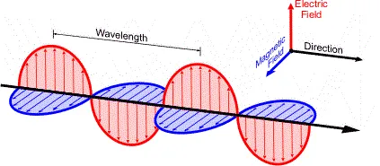
The proliferation of modern electronic devices has brought great convenience, but it has also worsened the electromagnetic environment. Electromagnetic interference (EMI) is a disturbance caused by the interaction between electromagnetic waves and electronic components.
When electronic devices operate, they generate electromagnetic waves that can interfere with each other, negatively impacting sensitive circuits. In severe cases, this can prevent circuits from functioning correctly. This is why reducing EMI is crucial for improving system stability. This article discusses how EMI affects consumer electronics and sensitive equipment, such as home appliances, alarm systems, and garage door openers.
How to Optimize EMI
In switching power supply design, circuit design and printed circuit board layout are two key aspects of solving EMI problems. In circuit design, the switching frequency and the ringing at the switch node are major sources of EMI.
Two effective methods for optimizing EMI are switching frequency control and anti-ringing control.
Switching Frequency Control
This method reduces EMI by extending the rise and fall times of the switching node, thereby lowering the dV/dt rate.
Anti-Ringing Control
Ringing on the switch node can lead to EMI issues. The more ringing a device exhibits, the worse its EMI performance will be. Adding a 1 kΩ resistor (R) and another switch (S1) between the SW node and GND can mitigate ringing. Under light load conditions, when both the high-side and low-side switches are off, S1 turns on, allowing a portion of the inductor (L1) current to be discharged to GND through R and S1.
PCB Layout for Improved EMI
The feedback signal of a switching power supply is a sensitive analog signal, susceptible to interference from its own switching signals. A good layout can reduce this EMI, whereas a poor layout can result in large ripple or even cause the power supply to fail.
Here are some tips for achieving better EMI performance through component placement and PCB layout:
- Place the input filter capacitor close to the IC.
- Use a shielded inductor.
- Use a small SW pad layout.
- Use a single-point connection for the IC GND and system GND.
- Keep the connection between the input ground and GND as short and wide as possible.
- Connect the ground of the VCC capacitor to the IC's ground through multiple vias or a wide trace.
- Keep the trace between the input capacitor and the IN pin as wide and short as possible.
- Ensure all feedback connections are direct and use short traces.
- Place feedback resistors and compensation components as close to the chip as possible.
- Keep the SW signal away from sensitive analog signals, such as the FB signal.
Optimization for Consumer and RF-Sensitive Applications
In a world full of electronic devices, from home appliances to consumer products and RF-sensitive equipment like garage door openers and alarm systems, EMI can cause unintended interactions and operational problems. The MP2317 series addresses this issue by optimizing EMI performance. These devices come in a simple package and support single-layer PCB designs, which simplifies manufacturing and reduces costs.
The MP2317 series can be used as a secondary-side DC/DC converter.
Key features of the MP2317 series include:
- Wide input voltage range from 7.5V to 26V.
- Low quiescent current of 150uA.
- Excellent load/line regulation and transient response.
- Efficiency up to 96%; reaches 80% at 12V to 5V/20mA.
- Comprehensive protection features (OTP, UVLO, OCP) for improved reliability and lifespan.
The MP2317, MP2344, and MP2345 series of 1A/2A/2.5A, 26V high-efficiency switching regulators from MPS use a small 6-pin SOT23 package with a large pin pitch (0.95mm). This package allows for single-layer PCB layout, simplifying the manufacturing process and saving costs. The three regulators in this series are pin-to-pin compatible, allowing system engineers to switch to a different current rating without changing the PCB, thus saving design time and cost.
The Importance of EMC in the Design Phase
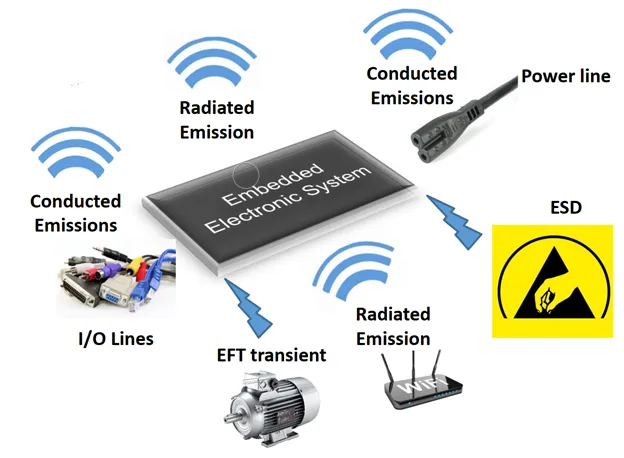
As electronic and electrical systems become more prevalent, EMC testing is a mandatory requirement for most products. However, EMC testing is expensive, and building an EMC lab is a major investment, as most of the measurement equipment must be imported. A product's EMC performance is determined during the design phase. If EMC considerations are ignored during design, a product is very likely to fail EMC testing, preventing it from meeting regulatory standards and obtaining certification.
For example, design engineers can implement effective filter circuits at the I/O interface to eliminate conducted noise at the system's entry point. Isolation circuits, such as transformer isolation and opto-isolation, can resolve conducted interference entering through power lines, signal lines, and ground wires, while also preventing interference from common impedance and long-line transmission. Energy absorption circuits can reduce the noise energy absorbed by circuits and components. By carefully selecting components and arranging the circuit system, the impact of interference can be minimized.
EMC Troubleshooting Tips
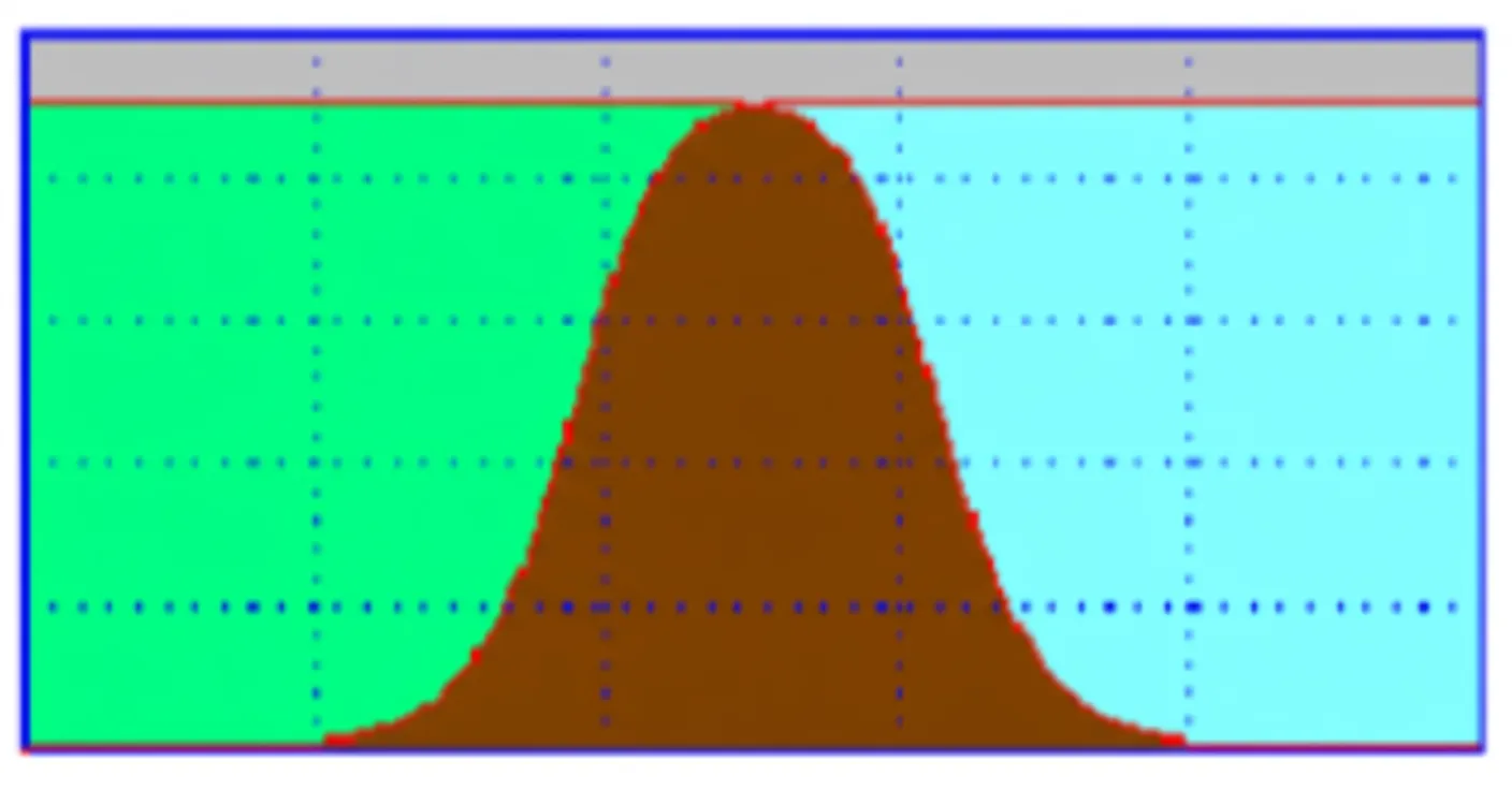
- Between 150 kHz and 1 MHz, interference is primarily differential-mode. From 1 MHz to 5 MHz, both differential-mode and common-mode interference are present. Above 5 MHz, it is almost entirely common-mode. Differential-mode interference can be caused by capacitive or inductive coupling. Generally, interference above 1 MHz is common-mode, while at lower frequencies, it is differential-mode. To estimate common-mode interference, you can connect a resistor and capacitor in series and place them in parallel with the Y-capacitor, then measure the voltage across the resistor with an oscilloscope.
- Add a differential-mode inductor or resistor after the fuse.
- For low-power supplies, a PI-type filter can be effective. It is advisable to use a larger electrolytic capacitor near the transformer.
- In a front-end PI EMI filter, the differential-mode inductor is only effective for low-frequency EMI. Do not choose an overly large one (DR8 is too big; a resistor type or DR6 is better), as it can worsen radiated emissions. If necessary, add a ferrite bead in series, as high-frequency noise tends to radiate directly to the front end rather than follow the traces.
- Conducted emissions in the 0.15 MHz - 1 MHz range may fail when the device is cold but pass with a 7 dB margin when hot. This is mainly due to a high DF (dissipation factor) value in the primary bulk capacitor. The ESR is higher when cold and lower when hot. The switching current across the ESR creates a switching voltage that causes a current to flow between the L and N lines, resulting in differential-mode interference. The solution is to use a low-ESR electrolytic capacitor or add a differential-mode inductor between two electrolytic capacitors.
- If tests consistently fail at 150 kHz, try increasing the X-capacitor value. If the interference level drops, it indicates differential-mode interference. If there is little change, it is likely common-mode interference. Alternatively, try winding the power cord a few times around a large magnetic ring. If the interference drops, it is common-mode. If the interference curve is clean at higher frequencies, try reducing the Y-capacitor value and check the board layout, or add a magnetic ring at the input.
- Increase the inductance of the single-winding inductor at the PFC input stage.
- Adjust the components in the PWM circuit to set the main frequency to around 60 kHz.
- Place a copper foil shield tightly against the transformer core.
- Asymmetrical windings in a common-mode choke (e.g., one side having one less turn) can cause conducted emissions failures in the 150 kHz - 3 MHz range.
- There are typically two main points for conducted emissions: around 200 kHz and 20 MHz, which reflect the circuit's performance. The 200 kHz peak is mainly due to spikes from leakage inductance, while the 20 MHz noise is from circuit switching. If not handled properly, the transformer can become a significant source of radiation that shielding cannot fix, causing radiated emissions to fail.
- Replace the input bulk capacitor with a low-ESR type.
- For power supplies without a Y-capacitor, wind the transformer by first winding the primary, then the auxiliary winding (wound tightly to one side), and finally the secondary.
- Add a resistor of a few kΩ to tens of kΩ in parallel with the common-mode choke.
- Shield the common-mode choke with copper foil and connect it to the ground of the bulk capacitor.
- In PCB design, keep the common-mode choke and the transformer separated to avoid mutual interference.
- Place a ferrite bead on the fuse lead.
- For three-wire inputs, reduce the capacitance of the Y-capacitors connecting the two input lines to ground from 2.2 nF to 470 pF.
- For designs with a two-stage filter, removing the second-stage 0.22uF X-capacitor can sometimes help, as X-capacitors in series can cause oscillations.
- In a PI filter circuit, if a bulk capacitor is laid flat on the PCB near the transformer, it can cause interference on the L-channel from 150 kHz to 2 MHz. To fix this, shield the capacitor with copper foil connected to ground, place a small PCB shield between the capacitor and transformer, or stand the capacitor upright. Alternatively, replace it with a smaller capacitor.
- As another solution to the previous point, replace the interfering bulk capacitor with a 1uF/400V or 0.1uF/400V capacitor and increase the value of the other capacitor.
- Add a small differential-mode inductor (a few hundred uH) before the common-mode choke.
- Wrap the switching transistor and its heatsink with copper foil, short the ends of the foil together, and connect it to ground with a wire.
- Shield the common-mode choke with copper foil and connect it to ground.
- Enclose the switching transistor in a metal shield connected to ground.
- Increasing the X2 capacitor value only helps in the 150 kHz range, not above 20 MHz. For high-frequency issues, add a nickel-zinc ferrite core (black magnetic ring) at the power input, with an inductance of about 50 uH to 1 mH.
- Increase the X-capacitor at the input.
- Increase the inductance of the input common-mode choke.
- Connect the auxiliary winding supply diode in reverse to ground.
- Use a taller, thinner electrolytic capacitor for the auxiliary winding supply filter or increase its capacitance.
- Increase the input filter capacitance.
- If conducted emissions fail in both the 150 kHz - 300 kHz and 20 MHz - 30 MHz ranges, add a differential-mode circuit before the common-mode circuit. Also, check for grounding issues. Ensure all ground connections are secure and that ground traces on the mainboard are routed smoothly without crossing over each other.
- When adding capacitors in parallel with a rectifier bridge, connect them between adjacent pins to address common-mode components, or between diagonal pins to address differential-mode components.
- Increase the input differential-mode inductance.
Common Sources of EMI in Electronic Products
- Switching circuits in switch-mode power supplies (SMPS): The fundamental frequency is tens to hundreds of kHz, with harmonics extending into the tens of MHz.
- Rectifier circuits in DC power supplies: The noise from linear power supply rectification can extend to several hundred kHz; for SMPS, high-frequency rectification noise can extend into the tens of MHz.
- Brush noise from DC motors: Noise frequency can extend to several hundred MHz.
- Operating noise from AC motors: Harmonics can extend into the tens of MHz.
- Interference from variable-frequency drive (VFD) circuits: The switching frequency of the control circuit can range from tens of kHz to tens of MHz.
- Switching noise from device state transitions: Noise from mechanical or electronic switches can have an upper frequency limit of several hundred MHz.
- Crystal oscillators and digital circuits in smart control devices: The fundamental frequency is tens of kHz to tens of MHz, with harmonics reaching several hundred MHz.
- Microwave leakage from microwave equipment: The fundamental frequency is in the GHz range.
- EMI from induction heating equipment: The fundamental frequency is tens of kHz, with harmonics extending to tens of MHz.
- Local oscillators and their harmonics in TV and audio receivers: The fundamental frequency is tens to hundreds of MHz, with harmonics reaching the GHz range.
- Digital processing circuits in information technology equipment and various automatic control systems: The fundamental frequency is tens to hundreds of MHz (and can reach several GHz after internal frequency multiplication), with harmonics extending to over ten GHz.
```