ALLPCB


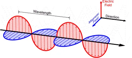
Sources of Electromagnetic Interference
Compared with linear regulators, switching power supplies offer higher efficiency, smaller size, and the ability to step up voltage. However, switching power supplies generate electromagnetic radiation during operation. Excessive radiation can disturb surrounding components and destabilize the system. To reduce radiation, it is important to understand the mechanisms and sources. In a switching converter the power switch charges the inductor when on and the inductor releases energy when the switch is off, enabling voltage conversion.
Because the power switch and the freewheeling diode are repeatedly switching on and off, the current is discontinuous. This changing current produces voltage spikes: from V = L * di/dt, the spike voltage equals the parasitic inductance in the switching current loop multiplied by the current slew rate. These spike voltages generate significant electromagnetic interference. Suppressing the spikes reduces EMI. The common mitigation methods are summarized below.
1. Shorten the Switching Current Loop
For a buck topology operating in continuous conduction mode, the switching current loops are as follows. When the power switch Q1 is on, the current loop is CIN → Q1 → L1 → COUT. When Q1 is off, the current loop is L1 → COUT → D1. Current through L1 and COUT is continuous, while the current through CIN, Q1, and D1 is switching current. The switching current generates spike voltages on the parasitic inductance of that loop. With di/dt unchanged, reducing the physical length of the CIN–Q1–D1 loop lowers the parasitic inductance and thus reduces radiated EMI.
2. Reduce the Current Slew Rate (di/dt)
Reducing the current slew rate reduces spike amplitude. If operating conditions and the current delta are fixed, the only way to reduce di/dt is to extend the duration of the current transition. One approach is to use a slower-switching diode to reduce the di/dt in the D1 loop. However, slower diodes such as slower recovery types increase diode loss, reduce efficiency, raise diode temperature, and can increase reverse leakage, negatively impacting system reliability.
3. Suppress High-Frequency Noise
Schottky diodes have parasitic capacitance, and the switching loop has parasitic inductance. Switching current flowing through D1 can cause ringing due to these parasitic inductance and capacitance. If the ringing frequency exceeds about 30 MHz, it falls into common radiated test bands and will be detected by test equipment. Placing a ferrite bead in series with the Schottky diode can filter high-frequency components and reduce radiated energy. Note that adding a ferrite bead in series with the Schottky can generate a larger negative spike voltage at the diode; the sum of input voltage and the absolute value of the spike must remain below the IC voltage rating to ensure reliability.
Note: Typical chip ferrite beads are composed of magnetic powder, nickel, and silver paste. At high frequency they present significant impedance and can absorb signals above about 30 MHz.
4. Add an RC Snubber
When intrinsic mitigation is insufficient, add external suppression components. A parallel RC snubber between the switch node and ground can absorb spike energy generated by parasitics and shift resonant frequency, reducing radiated emissions. Combining a ferrite bead in series with the Schottky and an RC snubber often yields better suppression. The typical circuit is shown below.
5. Add a Common-Mode Choke
Radiated test bands typically span 30 MHz to 1 GHz, corresponding to wavelengths from 0.3 m to 10 m. To effectively radiate at a given wavelength, a conductor typically needs to be at least one twentieth of that wavelength. Long output wiring can act as an antenna. Placing a common-mode choke in series with the output can filter common-mode currents and reduce radiation. However, common-mode chokes tend to be bulky, costly, and difficult to integrate, making them less suitable for very small or low-cost designs.
Practical Checklist
Use the following practical steps to help a switching power design pass radiated emission tests:
- Optimize PCB layout. Place the input capacitor close to the IC VIN and ground pins. Route feedback traces away from switching nodes. Surround switching nodes with ground traces and shorten the switching current loop. In practice, place the input capacitor positive terminal close to the IC VIN pin, the Schottky cathode close to the IC SW pin, and the Schottky anode close to the input capacitor negative terminal.
- Place a ferrite bead and an RC snubber at the Schottky diode. Choose a ferrite bead with AC impedance around 60–80 ohms; lower DC resistance reduces loss. For the RC snubber, use a resistor around 10 ohms and a capacitor below 1 nF.