ALLPCB


Introduction
Demand for wearable ECG devices for personal and remote health monitoring is increasing, bringing higher expectations for accuracy, reliability, and longer battery life. Designers face challenges because ECG readings are highly sensitive to motion and other interference sources, and much of the available battery power is consumed processing ECG signals.
To improve reliability and user experience, wearable designers need solutions that can extract, amplify, and filter small bioelectric potentials while consuming minimal power. New ECG heart-rate monitor ICs can play a central role in next-generation cardiac monitoring designs.
Understanding wearable ECG requirements
An electrocardiogram measures heart rhythm and helps diagnose cardiac issues including myocardial infarction, ischemia, and other abnormalities. ECG records the electrical activity generated by myocardial tissue. That activity produces voltages or bioelectric potentials that propagate to the skin. Although these potentials are in the microvolt range, they can be measured noninvasively and reliably using electrodes attached to the skin.
Professional ECG systems can use up to 10 electrodes on the chest and limbs. Wearable ECG systems, such as chest straps and smart shirts, use fewer electrodes and commonly employ two- or three-electrode configurations. This reduces system footprint and improves wearer comfort, but comfort must be balanced against accuracy and reliability.
Balancing those requirements is difficult because wearable applications present a variety of noisy environments that cause signal fluctuations. Even small body movements, such as chewing gum or facial expressions, can introduce noise. Since users wearing ECG-enabled devices are likely to be active, motion is a major noise source. Other factors include interference from mains power or other electrical equipment.
Another constraint for wearable ECG systems is limited battery capacity. For example, a high-end smartwatch with a 246 mAh, 3.78 V lithium-ion battery may run about 18 hours under mixed usage. Given the required communication and processing, efficient system design is essential.
To address noise and power issues, semiconductor suppliers now offer integrated circuits designed specifically for heart-rate monitoring in wearable devices.
ICs for wearable ECG
One such IC is Analog Devices' AD8233 ACBZ-R7, a fully integrated single-lead ECG front end. The AD8233 incorporates a dedicated instrumentation amplifier, an operational amplifier, a right-leg drive (RLD) amplifier, and a mid-supply reference buffer. It also features lead-off detection and an automatic rapid-recovery circuit that quickly restores the signal after electrode reconnection in mobile or active-user applications (see Figure 1).
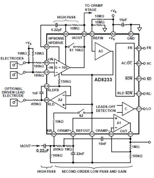
Figure 1: The AD8233 AFE integrates circuits required for wearable heart-rate monitor front ends, including lead-off detection and rapid recovery after reconnection. (Source: Analog Devices)
Noise mitigation
The AD8233 is designed to handle small bioelectric signals under noisy conditions and to produce outputs suitable for low-power analog-to-digital converters (ADCs).
To remove motion artifacts produced by physical activity, the AD8233 implements a two-pole high-pass filter. This filter also removes electrode half-cell potentials, which can pose a substantial challenge because their voltages are much higher than the bioelectric signals.
The AD8233 also integrates a general-purpose op amp that can implement three-pole low-pass filtering to further reduce noise. The RLD amplifier helps manage noise by improving common-mode rejection ratio (CMRR). It senses the common-mode voltage at the signal inputs and drives the patient with an inverted signal. This driven electrode function helps maintain a constant voltage between the patient and the AD8233, providing high CMRR.
Lead-off detection
To detect electrode connection status and alert the system if a failure occurs, the AD8233 includes lead-off detection circuitry. This is particularly useful in wearables where the user may be in motion.
Lead-off detection works in two- or three-electrode configurations and can operate while the device is in shutdown. The lead-off output can serve as a wake signal for the system microcontroller, saving overall power.
The AD8233 also includes a rapid-recovery feature that works with the lead-off detection. After sudden signal changes caused by a lead-off condition, rapid recovery allows the AD8233 to quickly restore operation when the electrodes are reconnected.
ECG board with AD8233
To help designers get started, the AD8233CB-EBZ evaluation board presents the AD8233 in a wearable ECG front-end design suitable for fitness applications. The default configuration is a three-electrode heart-rate monitoring system connected to the user's hands (see Figure 2).
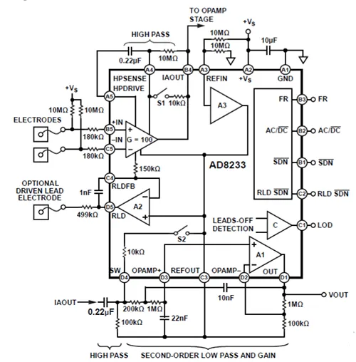
Figure 2: The standard AD8233CB-EBZ evaluation board supports a three-electrode heart-rate monitoring system. (Source: Analog Devices)
The board can connect directly to electrodes at the inputs and to an ADC at the output. Although the electrode terminals include series resistors, it is recommended to test the board first with an ECG signal generator rather than a live subject. Resistors alone are not a comprehensive patient-protection system and may not prevent transients or leakage currents from power lines or acquisition systems. For medical system design best practices and standards, start with IEC 60601.
When building an ECG system, gain and filtering may need adjustment to meet accuracy and electrode-placement considerations. Designers can tune the AD8233's two-pole high-pass filter and the integrated op amp cutoff frequencies by changing component values on the AD8233CB-EBZ.
By switching positions for input bias selection and electrodes on the AD8233CB-EBZ, the lead-off detection system can be configured for AC or DC two- and three-electrode modes. The rapid-recovery feature can also be enabled via a switch on the board.
To save battery, the AD8233 includes a shutdown pin. The AD8233CB-EBZ board also provides a standby switch that reduces AD8233 current consumption from a typical 50 μA to under 1 μA.
Building a wearable ECG device
Smart wearable medical devices can combine two or more functions, including heart-rate monitoring, pedometer and activity tracking, bioelectric potential measurement, bioimpedance, and SpO2 measurement.
In a typical design, the AD8233 serves as the ECG analog front end (AFE). The AFE connects to an analog-to-digital converter such as Analog Devices' AD7915 (see Figure 3).
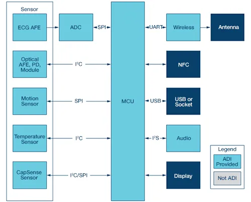
Figure 3: The AD8233 is a typical ECG AFE in a smart wearable design, providing inputs to a low-power ADC like the AD7915. (Source: Analog Devices)
The AD7915 is a 16-bit ADC designed for battery-powered medical applications. As with the AD8233, the AD7915 operates from a single supply, simplifying design. The ADC connects to the system microcontroller via an SPI port.
When selecting an MCU for primary processing and control, look for MCUs designed for low-power wearables, as they meet core requirements such as accuracy for vital-sign measurements, low power consumption, and a relatively comprehensive set of I/O like NFC, USB, display, and audio.
An example MCU optimized for these requirements is Analog Devices' ADuCM350, which is based on an ARM 32-bit Cortex-M3 processor. The IC is a high-precision integrated instrument for monitoring vital signs and performing current, voltammetry, and impedance measurements. The ADuCM350 can also be powered by a coin cell, saving space.
Combining AD8233 AFE and ADuCM350 MCU
To combine the AD8233 and ADuCM350 and obtain ECG signals, run both ICs from the same 3.3 V supply using the AD8233 evaluation board (see Figure 4).
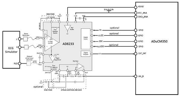
Figure 4: Combining the AD8233 with the ADuCM350 enables bioimpedance and ECG measurements. (Source: Analog Devices)
The first step is to calibrate the AD8233 AFE within the system to ensure the two-IC combination does not degrade the specified 9.8 μV p-p noise performance. Short the +IN and -IN pins and connect them to VBIAS. Determine the maximum peak-to-peak noise variation and divide it by the AD8233 gain (1,100). The result should be around 5.8 μV p-p.
Next, connect AD8233_REFIN to VBIAS on the ADuCM350 and apply an ECG generator to +IN, -IN, and RLD on the AD8233. With the ECG generator set to 60 BPM, the output should resemble Figure 5.
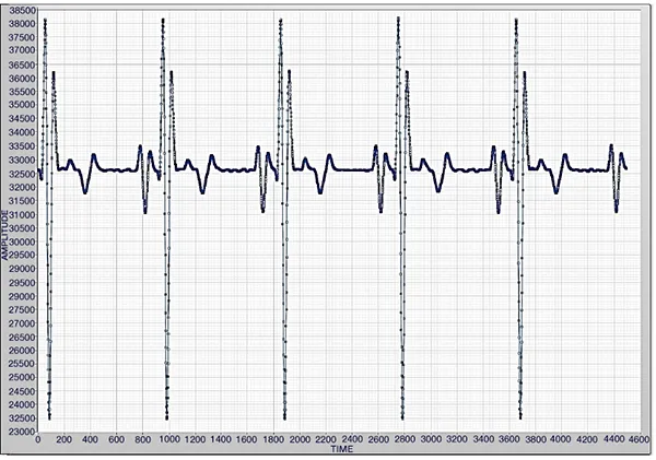
Figure 5: With the ECG generator set to 60 BPM, the heart-rate monitor output should indicate compatibility between components and the system. (Source: Analog Devices)
Conclusion
Wearable devices introduce challenges for ECG implementation, including noise and power constraints. However, ECG heart-rate monitor ICs and evaluation boards designed for this application are increasingly available and well supported. These tools enable engineers to develop systems that provide accurate, low-power, and reliable heart-rate monitoring in wearable electronics.