 ALLPCB


Introduction
Flex PCBs represent a critical advancement in electronics, enabling compact designs in applications like wearables, medical devices, and automotive sensors where space constraints demand bendable interconnects. Depaneling these flexible circuits from production panels marks the final manufacturing step, yet it poses unique challenges due to their thin substrates and susceptibility to mechanical stress. Improper handling during flex PCB depaneling can lead to creasing, tearing, or delamination, compromising electrical performance and yield rates in high-volume production. Specialized depaneling machines address these issues by incorporating precise material handling features such as vacuum fixturing and controlled tension systems. This guide explores the technical principles, methods, and best practices for depaneling thin PCBs, emphasizing factory-driven approaches aligned with industry standards. Engineers benefit from understanding these processes to optimize designs for reliable separation without post-process defects.
Flex circuits, often constructed from polyimide or similar materials, require gentle separation to maintain integrity throughout their lifecycle. Factories prioritize machines that minimize heat-affected zones and particulate generation, ensuring compliance with qualification specifications like IPC-6013. As production scales, selecting the right depaneling technology becomes essential for balancing throughput and quality.
What Is Flex PCB Depaneling and Why It Matters
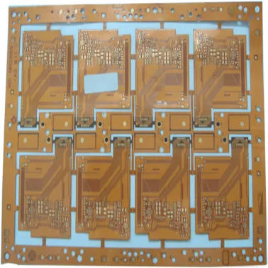
Flex PCB depaneling involves singulating individual flexible circuits from a multi-unit production panel after lamination, etching, and coverlay application. Unlike rigid boards, flex panels lack structural rigidity, making traditional breakaway methods impractical and prone to inducing micro-cracks in copper traces. This process directly impacts material handling, as operators or automated systems must secure the thin substrates without applying excessive force that could warp or stretch the material. In factory environments, effective depaneling ensures high first-pass yields, reducing rework and scrap associated with handling flexible circuits.
The relevance stems from the growing demand for lightweight, conformable electronics in dynamic environments. Poor depaneling techniques can introduce residual stresses that manifest as failures during subsequent flexing or thermal cycling. Adhering to standards like IPC-6013 for performance qualification helps verify that depaneled flex PCBs meet mechanical and electrical requirements post-separation. Engineers designing for manufacturability must consider depaneling early to avoid costly panelization errors.
Material handling during this phase prevents contamination from cutting debris, which could migrate into fine-pitch features. Factories report that optimized depaneling workflows enhance traceability and support lean manufacturing principles.
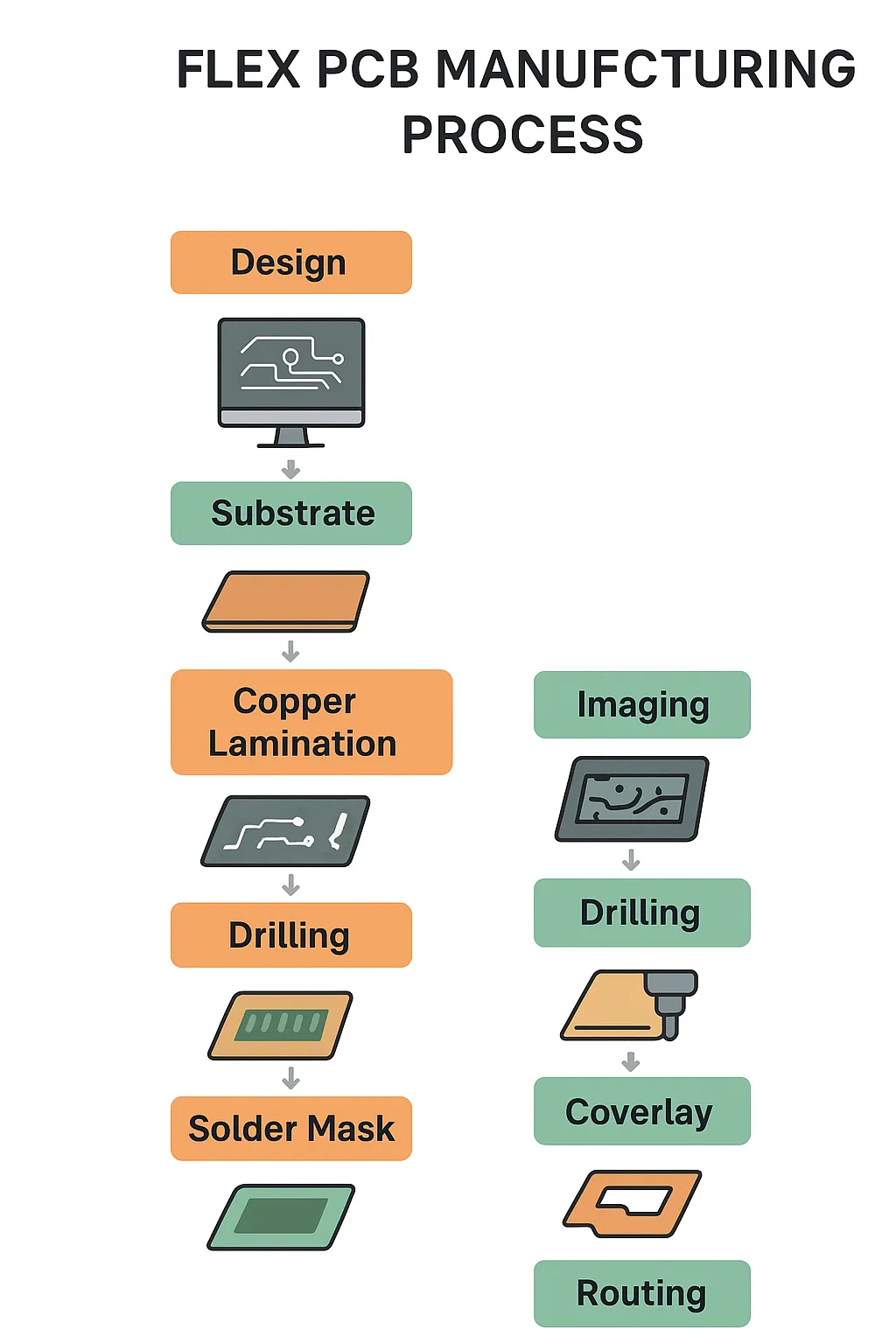
Technical Principles of Depaneling Methods for Flex PCBs
Several depaneling approaches exist, but their suitability for flex circuits hinges on minimizing mechanical and thermal stresses. Mechanical routing uses a high-speed spindle with carbide bits to mill along scored or tabbed outlines, yet this method generates vibration and burrs that damage thin flex materials. Punching or die-cutting applies shear force through matched tooling, suitable for thicker substrates but risking tearing in flex due to uneven stress distribution. These contact-based techniques demand robust fixturing to immobilize the panel, often using adhesive tapes or vacuum tables tailored for flexible circuits.
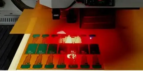
Laser depaneling flex PCB emerges as the preferred non-contact method, employing focused beams to ablate material along predefined paths. UV lasers excel at polyimide substrates with minimal heat spread, while CO2 or fiber lasers handle coverlay layers through controlled pulse durations. The process relies on galvo scanners for precise beam steering, enabling complex contours without physical tooling changes. Alignment systems, often vision-based, ensure sub-micron accuracy critical for handling thin PCBs.
Key to laser mechanisms is the interaction between wavelength and material absorption. For instance, shorter wavelengths vaporize dielectrics cleanly, reducing charring that could affect adhesion layers. Factory setups integrate exhaust systems to evacuate fumes and particulates, maintaining cleanroom compatibility. These principles align with design standards like IPC-2223, which guide outline geometries to facilitate stress-free separation.
Material Handling Techniques in Flex PCB Depaneling Machines
Effective material handling distinguishes reliable depaneling machines for flex PCBs, focusing on securing panels without distortion. Vacuum-assisted fixturing uses porous tables or zoned chucks to hold panels flat, countering natural curl from thin substrates. Tension control mechanisms apply uniform pull to prevent slack during routing or laser passes, ensuring consistent cut quality across the panel. Automated loaders with soft-touch grippers transfer panels between stations, minimizing human intervention and handling flexible circuits delicately.
For laser depaneling flex PCB, machines incorporate dynamic focusing to accommodate panel warpage, maintaining optimal beam-to-surface distance. Dust collection integrates inline HEPA filtration, capturing nano-scale particles that could contaminate solder pads. Cooling systems, such as air knives or cryogenic assists, mitigate localized heating in sensitive areas. These features enable high-throughput processing while preserving flex integrity.
Panel orientation plays a pivotal role; factories orient flex panels with bend axes parallel to feed directions to avoid torque. Software-driven nesting optimizes layout, reducing waste and simplifying handling paths. Engineers should specify handling tolerances in design files to match machine capabilities.
Multi-axis manipulators further enhance precision, allowing 3D contour following for rigid-flex hybrids. Overall, these techniques ensure depaneling thin PCBs aligns with production scalability.
Best Practices for Depaneling Thin PCBs and Handling Flexible Circuits
Start with panelization strategies that support gentle depaneling, such as fiducials for alignment and minimal tabs to reduce shear points. Select laser systems with adjustable parameters: pulse frequency around material resonance, power scaled to substrate thickness, and scan speeds calibrated to avoid overheating. Pre-depaneling inspections verify panel flatness, rejecting warped lots that complicate handling flexible circuits. Factories implement inline metrology to monitor cut quality, flagging anomalies like incomplete ablation.
Operator training emphasizes ESD-safe handling and proper fixturing sequences to prevent static-induced damage. Maintenance schedules for optics and exhausts sustain performance, with calibration per manufacturer guidelines. For high-mix production, modular machines allow quick recipe changes, optimizing flex PCB depaneling runs.
Integrate depaneling into the broader workflow: post-cut cleaning via ionized air or ultrasonics removes residues before stacking. Data logging tracks parameters for process optimization, supporting continuous improvement. These practices, informed by IPC-6013 qualification tests, elevate factory reliability.
Collaborate with manufacturing early to validate designs, simulating stresses via FEA if needed. Yield monitoring post-depaneling quantifies effectiveness.
Common Challenges and Solutions in Flex PCB Depaneling
Thin flex substrates warp under humidity or thermal gradients, complicating fixturing and leading to misalignment during laser depaneling flex PCB. Solution: precondition panels in controlled environments and use adaptive clamping. Heat-affected zones cause coverlay discoloration or trace lift-off; mitigate with optimized laser parameters and assist gases. Particulate adhesion risks shorts in fine features, addressed by enhanced vacuum and contactless transport.
Alignment drift from panel flexure demands robust vision systems with multiple fiducials. For dynamic flex areas, staged depaneling separates rigid sections first, easing handling. Troubleshooting logs help correlate defects to root causes, refining processes iteratively.
These solutions ensure robust production.
Conclusion
Depaneling machines for flex PCBs demand precision material handling to safeguard thin, bendable circuits from damage. Laser methods outperform mechanical alternatives by delivering clean, stress-free cuts, while advanced fixturing and controls optimize factory workflows. Adhering to standards like IPC-6013 and IPC-2223 guides reliable outcomes. Engineers gain from proactive design and process integration, achieving higher yields and performance. As flex applications expand, mastering these techniques remains key to innovation.
FAQs
Q1: What is flex PCB depaneling, and why is it challenging for thin materials?
A1: Flex PCB depaneling separates individual flexible circuits from production panels using methods like laser cutting to avoid mechanical stress. Thin substrates crease or tear easily under traditional routing or punching, demanding specialized machines with vacuum fixturing. Proper handling flexible circuits prevents warpage and maintains trace integrity per IPC standards. Factories prioritize non-contact processes for high yields.
Q2: What are the best practices for handling flexible circuits during depaneling?
A2: Secure panels with zoned vacuum tables and tension controls to flatten thin flex without distortion. Use vision alignment and dynamic focusing for precise paths, especially in laser depaneling flex PCB. Precondition environments to minimize warpage, and integrate dust extraction for cleanliness. Monitor parameters inline to sustain quality in production runs.
Q3: Why choose laser depaneling for thin PCBs over mechanical methods?
A3: Laser depaneling flex PCB offers non-contact precision, minimizing stress and burrs that damage delicate flex materials. Mechanical routing induces vibration leading to micro-cracks, unsuitable for thin substrates. Lasers provide clean edges with adjustable heat control, supporting complex outlines. This aligns with factory needs for reliability and throughput.
Q4: How do depaneling machines improve material handling for flex circuits?
A4: Machines feature soft grippers, automated loaders, and adaptive fixturing to gently manage flexible circuits without creasing. Exhaust and cleaning integrate seamlessly, reducing contamination risks. Software optimizes nesting and recipes for efficiency. These enhance depaneling thin PCBs, boosting overall process control.


