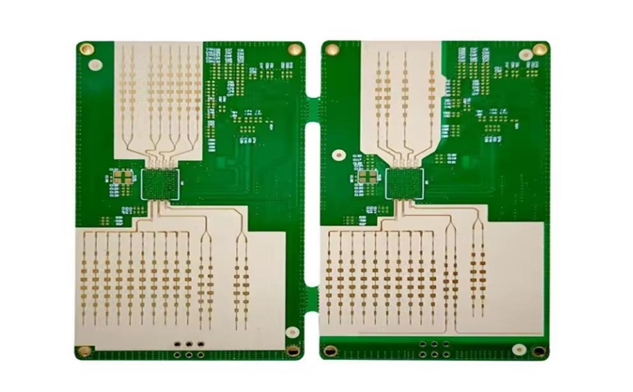
If you're looking to improve PCB manufacturing efficiency and reduce costs, PCB panelization is the key. This process involves arranging multiple printed circuit boards (PCBs) on a single panel for production, streamlining fabrication and assembly while minimizing waste. In this comprehensive guide, we'll dive deep into PCB panelization, covering its benefits, design tips, and techniques to help you achieve cost-effective PCB assembly. Whether you're a designer or manufacturer, you'll find actionable insights to optimize your workflow.
What Is PCB Panelization and Why Does It Matter?
PCB panelization is the practice of grouping several individual PCBs onto a larger panel for manufacturing. Instead of producing each board separately, multiple designs are fabricated and assembled as a single unit, then separated into individual boards after production. This method is widely used in high-volume production to save time, reduce costs, and improve handling during automated assembly processes.
The importance of panelization lies in its ability to enhance efficiency. By processing multiple boards at once, manufacturers can cut down on machine setup times and material waste. For small or irregularly shaped PCBs, panelization ensures stability during production, preventing damage and ensuring consistent quality. As a bonus, it often lowers labor costs by simplifying the assembly process.
Key Benefits of PCB Panelization
Understanding the advantages of PCB panelization can help you make informed decisions during the design and manufacturing stages. Here are the primary benefits that make this technique a game-changer for cost-effective PCB assembly:
- Cost Reduction: Panelization minimizes material waste by maximizing the use of the panel space. For instance, a standard panel size of 18x24 inches can often accommodate dozens of small PCBs, reducing the per-unit cost of raw materials by up to 30% in some cases.
- Improved Manufacturing Efficiency: Processing a single panel instead of individual boards cuts down on machine handling time. This can reduce production lead times by 20-40%, depending on the complexity of the design.
- Better Quality Control: Handling a panel during assembly reduces the risk of damage to individual boards, especially for delicate or small designs. It also ensures uniformity in soldering and component placement across all boards.
- Simplified Assembly: Automated pick-and-place machines and reflow ovens work more efficiently with panels, as they can process multiple boards in one go. This reduces labor costs and speeds up the assembly process.
- Support for Small or Irregular Designs: Tiny or non-rectangular PCBs are difficult to handle individually. Panelization provides a stable framework, making them easier to fabricate and assemble without errors.
Types of PCB Panelization Techniques
There are several methods to panelize PCBs, each suited to different designs and production needs. Choosing the right technique is crucial for balancing efficiency and ease of separation. Below are the most common approaches:
1. V-Cut Panelization
V-Cut, also known as V-Scoring, involves creating shallow grooves along the separation lines of individual boards. These grooves allow the boards to be snapped apart manually after assembly. This method is ideal for rectangular boards and is widely used due to its simplicity and low cost. However, it’s not suitable for complex or fragile designs, as the snapping process can cause stress to components near the edges.
2. Tab Routing
Tab routing uses small, breakable tabs to hold individual boards together within the panel. After assembly, the boards are separated by cutting or breaking the tabs. This method is more flexible than V-Cut and works well for irregular shapes. However, it may leave small protrusions on the board edges, which might require additional finishing.
3. Perforated Tabs
Similar to tab routing, perforated tabs use a series of small holes along the separation lines to create weak points for easy breaking. This technique is often used when clean edges are not critical, as it can leave rough spots after separation. It’s a cost-effective option for simpler designs.
4. Combination Methods
For complex projects, a mix of V-Cut and tab routing can be used. For example, straight edges might use V-Scoring for clean separation, while curved or irregular edges rely on tabs for stability. This hybrid approach offers flexibility but may increase production complexity.
PCB Panel Design Guidelines for Optimal Results
Effective PCB panel design is essential for maximizing the benefits of panelization. Poor design can lead to wasted space, damaged boards, or assembly errors. Here are some key guidelines to follow when creating a panel layout:
- Panel Size Compatibility: Ensure the panel size matches the capabilities of your manufacturing equipment. Most automated machines, such as SMT pick-and-place systems, handle panels between 50x50mm and 450x330mm. Check with your manufacturer for exact specifications.
- Spacing Between Boards: Leave adequate spacing (typically 2-3mm) between individual boards to allow for separation without damaging components. For V-Cut, ensure a minimum groove width of 0.3mm for clean snapping.
- Edge Rails: Add process edges or rails (usually 5-10mm wide) around the panel to provide stability during handling and assembly. These rails can also include fiducial marks for machine alignment.
- Component Placement: Avoid placing components too close to board edges (maintain at least 1.5mm clearance) to prevent damage during separation. For surface-mount components near edges, consider using tab routing instead of V-Cut to reduce stress.
- Panel Utilization: Maximize the number of boards per panel to reduce material costs, but avoid overcrowding. Aim for at least 80-90% panel utilization while maintaining necessary spacing and rails.
How PCB Panelization Boosts Manufacturing Efficiency
One of the standout advantages of PCB panelization is its impact on manufacturing efficiency. By processing multiple boards simultaneously, every stage of production becomes faster and more streamlined. Let’s break down how this works:
- Fabrication Stage: Etching, drilling, and plating processes are performed on a single panel, reducing setup times. For example, drilling 100 holes on a panel of 10 boards takes far less time than drilling 10 holes on 10 individual boards.
- Assembly Stage: Automated assembly equipment, like pick-and-place machines, can place components on multiple boards in one cycle. This can cut assembly time by 30-50% for high-volume runs.
- Testing Stage: Testing multiple boards at once, such as through Automated Optical Inspection (AOI), ensures consistency and reduces manual handling. This can improve defect detection rates by up to 25%.
These efficiency gains translate directly into shorter lead times and lower production costs, making panelization a must for scalable manufacturing.
Cost-Effective PCB Assembly with Panelization
Cost-effective PCB assembly is a top priority for any project, and panelization plays a critical role in achieving this goal. By optimizing material usage and reducing labor, panelization can significantly lower the overall cost per board. Here’s how:
- Material Savings: A well-designed panel minimizes scrap material. For instance, arranging 20 small boards (each 2x2 inches) on an 18x24-inch panel uses nearly 90% of the material, compared to only 50% if produced individually.
- Reduced Labor Costs: Handling one panel instead of dozens of individual boards cuts down on manual labor. This can save up to 40% on labor costs for large orders.
- Fewer Machine Cycles: Running a single panel through fabrication and assembly equipment reduces machine wear and energy consumption, further lowering costs.
By focusing on smart panel design and choosing the right separation method, you can achieve substantial savings without compromising quality.
Common Challenges in PCB Panelization and How to Avoid Them
While PCB panelization offers numerous benefits, it’s not without challenges. Being aware of potential pitfalls can help you avoid costly mistakes. Here are some common issues and solutions:
- Board Damage During Separation: Snapping or cutting can stress components near edges. Solution: Use tab routing for delicate designs and maintain a 2mm clearance for components near separation lines.
- Incompatible Panel Sizes: Panels that don’t match equipment specs can cause delays. Solution: Confirm panel dimensions with your manufacturer before finalizing the design.
- Wasted Space: Poor layout planning can lead to unused panel areas. Solution: Use design software to optimize board arrangement and aim for high panel utilization.
- Alignment Errors: Misaligned boards can lead to assembly issues. Solution: Include fiducial marks on edge rails for precise machine alignment.
Tools and Software for PCB Panelization
Designing a panelized PCB layout is easier with the right tools. Many PCB design software platforms offer built-in panelization features to help you arrange boards, add separation lines, and optimize spacing. These tools often include simulation capabilities to test panel stability and manufacturability before production.
Popular software options include features to export panel designs in standard formats like Gerber files, ensuring compatibility with manufacturing processes. When choosing a tool, look for one that supports custom panel sizes, automated spacing adjustments, and integration with fabrication requirements.
Best Practices for a Successful PCB Panelization Tutorial
For those new to PCB panelization, following best practices can make the process smoother. Here’s a quick tutorial summary to guide you:
- Start with Design Planning: Determine the number of boards per panel based on size and production volume. Use software to create a mock layout.
- Choose a Separation Method: Select V-Cut for simple rectangular boards or tab routing for irregular shapes. Consider component placement when deciding.
- Add Necessary Features: Include edge rails, fiducial marks, and adequate spacing to ensure stability and alignment.
- Verify with Manufacturer: Share your panel design files with your production team to confirm compatibility with their equipment and processes.
- Test a Prototype: Before full production, run a small batch to identify any issues with separation or assembly.
Conclusion: Unlock the Power of PCB Panelization
PCB panelization is a powerful strategy for boosting manufacturing efficiency and achieving cost-effective PCB assembly. By grouping multiple boards on a single panel, you can save on materials, reduce labor costs, and streamline production processes. Whether you're working on small prototypes or high-volume runs, mastering PCB panel design can transform your workflow.
With the right techniques, tools, and guidelines, panelization becomes a straightforward way to optimize your projects. Focus on smart layout planning, choose the best separation method for your design, and always collaborate with your manufacturing team for seamless results. By implementing the tips in this guide, you’ll be well on your way to cutting costs and enhancing efficiency in every PCB project.
 ALLPCB


