 ALLPCB


In the world of printed circuit board (PCB) manufacturing, ensuring the integrity of traces is critical for reliable performance. While visual inspection can catch obvious flaws like scratches or breaks on the surface, hidden trace defects—buried deep within multilayer boards or under components—often go undetected. So, how do you find these elusive issues without damaging the board? Advanced techniques like X-ray PCB inspection, thermal imaging PCB analysis, TDR trace analysis, impedance testing PCB, and non-destructive PCB testing provide the solution. In this blog, we’ll dive deep into these methods, explaining how they work, when to use them, and why they’re essential for high-quality PCB production.
Why Visual Inspection Isn’t Enough for Modern PCBs
Visual inspection, whether done by eye or with automated optical inspection (AOI) systems, is a great starting point. It can spot surface-level issues like misaligned components or visible trace breaks. However, modern PCBs are often complex, with multiple layers, fine-pitch components, and traces as narrow as 0.1 mm. Defects like internal shorts, cracked vias, or hidden voids in solder joints are invisible to the naked eye or even high-resolution cameras. These flaws can lead to intermittent failures or complete board malfunction, costing time and money. That’s where advanced, non-destructive testing methods come in, allowing engineers to peer beneath the surface and catch problems before they escalate.
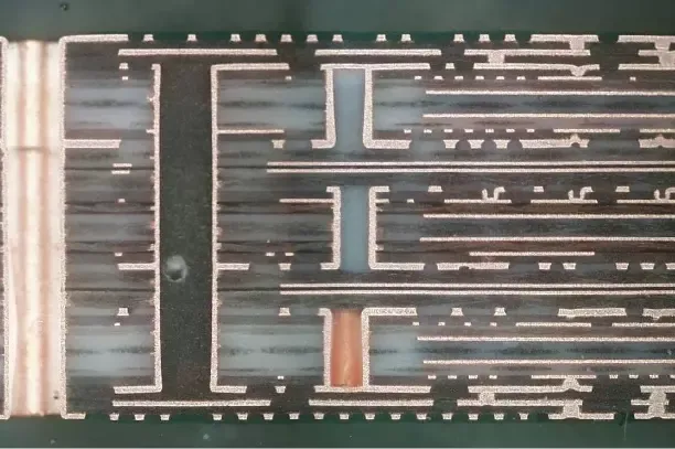
1. X-Ray PCB Inspection: Seeing Through the Layers
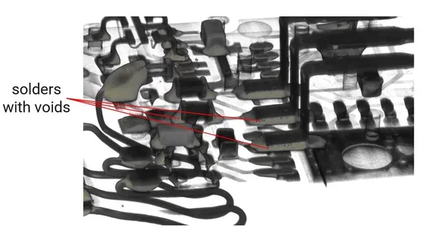
X-ray PCB inspection is a powerful non-destructive testing method that uses high-energy rays to penetrate the board and reveal internal structures. This technique is especially useful for multilayer PCBs where traces and vias are hidden between layers or under components like Ball Grid Arrays (BGAs). By generating detailed 2D or even 3D images, X-ray inspection can detect issues such as:
- Voids in solder joints (e.g., a void larger than 25% of the joint area is often flagged as a defect).
- Cracked or misaligned vias in internal layers.
- Hidden shorts or opens beneath fine-pitch components with lead spacing as small as 0.5 mm.
For example, consider a 6-layer PCB that fails intermittently due to a suspected via issue. X-ray inspection can pinpoint a hairline crack in the via barrel caused by thermal stress during soldering, allowing engineers to address the root cause without destroying the board. This method is non-invasive, meaning the PCB remains fully functional after testing, making it ideal for both prototyping and quality control in production.
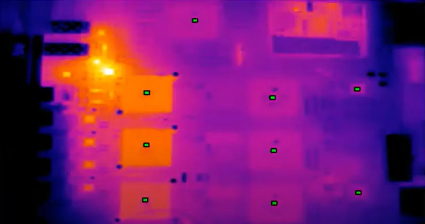
2. Thermal Imaging PCB: Detecting Heat Signatures of Defects
Thermal imaging PCB analysis is another non-destructive technique that uses infrared cameras to detect temperature variations across the board. When a PCB is powered on, defective traces or components often generate abnormal heat due to increased resistance or short circuits. For instance, a partially broken trace might cause a localized hotspot as current struggles to flow through the damaged area. Thermal imaging can identify:
- Hotspots caused by high-resistance trace defects.
- Short circuits that lead to excessive current flow and heat buildup.
- Poor thermal dissipation in densely packed areas of the board.
This method is particularly useful during functional testing. Imagine a PCB under load where a hidden trace defect causes a temperature spike of 10°C above the surrounding area. A thermal camera with a resolution of 0.1°C can easily detect this anomaly, guiding engineers to the exact location for further investigation. It’s a fast, contactless way to spot issues without disassembling the board.
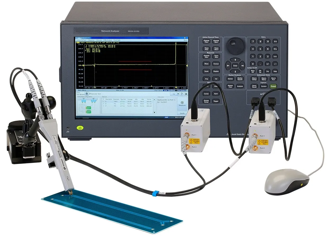
3. TDR Trace Analysis: Mapping Signal Integrity Issues
Time Domain Reflectometry (TDR) trace analysis is a specialized technique for evaluating the integrity of traces by measuring signal reflections. TDR works by sending a high-speed electrical pulse down a trace and analyzing the reflected signal to detect discontinuities. If there’s a break, short, or impedance mismatch along the trace, the reflection pattern will show anomalies at specific distances. Key applications include:
- Locating open circuits or breaks in traces with precision down to a few millimeters.
- Identifying shorts between adjacent traces or layers.
- Detecting manufacturing defects like over-etching that alter trace geometry.
For high-speed designs, where signal integrity is crucial, TDR can measure delays and pinpoint defects on traces carrying signals at speeds exceeding 1 GHz. For instance, if a trace break occurs 50 mm from the test point, TDR can map this location based on the time it takes for the signal to reflect back. This method is non-destructive and highly accurate, making it invaluable for debugging complex boards.
4. Impedance Testing PCB: Ensuring Electrical Consistency
Impedance testing PCB is a critical method for verifying that traces maintain consistent electrical characteristics, especially in high-frequency applications. Impedance mismatches—caused by manufacturing variations, trace damage, or improper material selection—can lead to signal distortion or loss. This test measures the opposition to alternating current along a trace, typically targeting values like 50 ohms or 100 ohms for specific designs.
Using tools like vector network analyzers (VNAs), engineers can test impedance across a frequency range (e.g., 100 MHz to 5 GHz) to ensure traces meet design specifications. A deviation of just 10% from the target impedance can cause significant signal reflection, leading to data errors in high-speed circuits. Common issues detected include:
- Trace width inconsistencies due to etching errors.
- Dielectric material variations affecting signal propagation.
- Hidden cracks or thinning in traces that alter electrical properties.
Impedance testing is non-destructive and often performed alongside TDR to provide a complete picture of trace health. It’s a must for PCBs in telecommunications or automotive systems where reliability is non-negotiable.
5. Non-Destructive PCB Testing: A Broader Approach
Non-destructive PCB testing encompasses a range of techniques, including the methods mentioned above, to evaluate board quality without causing damage. Beyond X-ray, thermal imaging, TDR, and impedance testing, other approaches like acoustic microscopy and eddy current testing can also detect hidden defects. Acoustic microscopy, for example, uses ultrasonic waves to identify delamination or voids within layers, while eddy current testing can spot conductivity issues in traces.
The beauty of non-destructive testing is its ability to preserve the PCB for further use or analysis. Whether you’re dealing with a prototype or a high-volume production run, these methods help maintain quality without sacrificing boards to destructive cross-sectioning or other invasive tests. They are especially critical in industries like aerospace or medical devices, where even a single defect can have catastrophic consequences.
When to Use Each Technique: A Practical Guide
Choosing the right inspection method depends on the type of defect, PCB complexity, and stage of production. Here’s a quick breakdown to guide your decision:
- X-Ray PCB Inspection: Best for multilayer boards with hidden vias or solder joints under components. Use during quality control after assembly.
- Thermal Imaging PCB: Ideal for functional testing under load to spot heat-related defects. Use during prototyping or failure analysis.
- TDR Trace Analysis: Perfect for high-speed designs needing precise defect location. Use during design validation or post-manufacturing testing.
- Impedance Testing PCB: Essential for high-frequency applications to ensure signal integrity. Use during manufacturing and final testing.
- Non-Destructive PCB Testing: A catch-all for various methods; select based on specific defect concerns and industry standards.
By combining these techniques, manufacturers can achieve a comprehensive inspection process that catches both surface and hidden defects, ensuring the highest reliability.
The Benefits of Advanced Inspection for PCB Reliability
Investing in advanced inspection techniques offers several advantages over relying solely on visual methods. First, they reduce the risk of field failures by catching defects early. A single undetected trace issue in a consumer device could lead to costly recalls or warranty claims. Second, these methods save time by pinpointing exact defect locations, eliminating guesswork during debugging. Finally, non-destructive approaches preserve valuable prototypes and production units, keeping costs down.
For instance, using X-ray inspection to detect a void in a BGA solder joint before shipping can prevent a failure that might occur after 1,000 hours of operation. Similarly, TDR trace analysis can ensure a high-speed data line maintains integrity, avoiding signal loss that could disrupt a critical system. These techniques are not just tools—they’re essential for meeting the demands of today’s high-performance electronics.
Conclusion: Elevating PCB Quality with Advanced Techniques
Finding hidden trace defects requires going beyond visual inspection to embrace advanced, non-destructive methods like X-ray PCB inspection, thermal imaging PCB analysis, TDR trace analysis, impedance testing PCB, and broader non-destructive PCB testing. Each technique offers unique strengths, from peering into internal layers with X-rays to mapping signal integrity with TDR. By integrating these approaches into your quality control process, you can ensure that every PCB meets the highest standards of reliability and performance.
At ALLPCB, we’re committed to supporting engineers with cutting-edge solutions for PCB manufacturing and testing. Whether you’re tackling a complex multilayer design or a high-speed application, leveraging these advanced inspection techniques will help you deliver flawless products to your customers. Stay ahead of defects—go beyond the surface and uncover what’s hidden.


