ALLPCB


Are you looking to understand the best silkscreen design techniques for your printed circuit board (PCB) projects? When it comes to precision and quality in PCB manufacturing, two advanced methods stand out: Liquid Photo Imaging (LPI) and Direct Legend Printing (DLP). In this comprehensive guide, we’ll dive deep into the LPI silkscreen process, explore the DLP silkscreen advantages, and provide a detailed comparison of LPI and DLP for PCB silkscreen design. Whether you’re an engineer, designer, or hobbyist, this post will help you choose the right technique for your needs.
What Is PCB Silkscreen and Why Does It Matter?
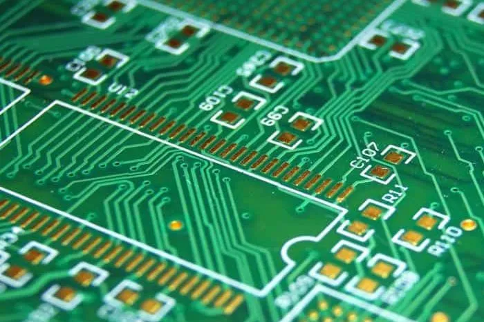
Before we compare the two advanced techniques, let’s start with the basics. PCB silkscreen is the layer of text, symbols, and markings printed on the surface of a circuit board. This layer serves as a guide for component placement, assembly instructions, and identification of parts like resistors, capacitors, and ICs. It’s often printed in white ink (though other colors are available) on top of the solder mask, ensuring visibility and clarity.
A high-quality silkscreen is crucial for reducing errors during assembly and troubleshooting. Poorly printed or unclear markings can lead to misplaced components or confusion during repairs. That’s why choosing the right silkscreen method is vital for both functionality and efficiency in PCB production.
Overview of Silkscreen Printing Techniques
Historically, silkscreen printing on PCBs was done manually using stencils to apply ink directly onto the board. While this method was cost-effective, it lacked precision and consistency, especially for intricate designs. Today, advanced techniques like LPI and DLP have revolutionized the process, offering higher accuracy and finer details. Let’s explore each method in detail to understand how they work and what benefits they bring to PCB manufacturing.
Liquid Photo Imaging (LPI): Precision Through Photochemical Processes
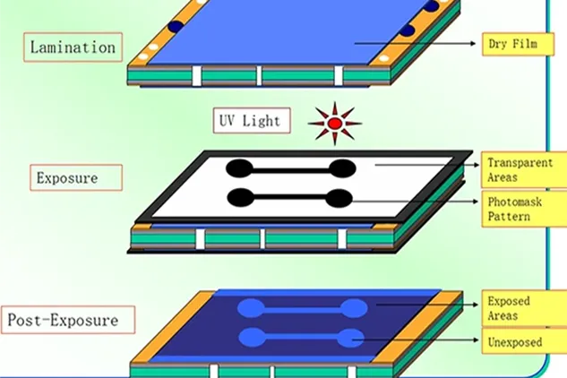
The LPI silkscreen process is a widely used technique that offers improved accuracy over traditional manual methods. It is especially effective for designs requiring line widths greater than 4 mils (0.004 inches). Here’s how it works:
- Application: A liquid photo-imageable epoxy is coated onto the PCB surface, similar to how solder mask is applied.
- Exposure: The coated board is exposed to ultraviolet (UV) light through a photomask, which defines the areas where the silkscreen markings will appear.
- Development: After exposure, the unexposed epoxy is washed away, leaving behind the desired markings.
- Curing: The board is then cured to harden the remaining epoxy, ensuring durability during assembly and use.
The LPI process is known for its ability to produce legible and consistent markings, even on complex boards with dense component layouts. It’s a step up from manual screen printing in terms of precision and is often used in medium to high-volume production runs.
Key Benefits of LPI:
- High accuracy for line widths as small as 4 mils, making it suitable for detailed designs.
- Consistent results across multiple boards, reducing variability in production.
- Cost-effective for medium-scale projects compared to more advanced methods.
Limitations of LPI:
- Not as precise as some newer techniques for ultra-fine markings (below 4 mils).
- Requires additional processing steps, which can increase production time.
Direct Legend Printing (DLP): Cutting-Edge Digital Precision
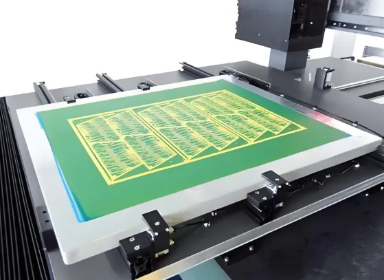
Direct Legend Printing (DLP) represents the pinnacle of silkscreen technology, leveraging digital printing methods for unparalleled accuracy. This method is ideal for intricate designs and high-density PCBs. Here’s a breakdown of the DLP silkscreen process:
- Digital Application: An inkjet printer, guided by CAD data, directly applies acrylic ink onto the PCB surface.
- UV Curing: As the ink is printed, it is immediately cured using UV light, ensuring it adheres firmly to the board.
- Precision Control: Since the process is driven by digital files, there’s no need for physical masks or stencils, allowing for rapid adjustments and customization.
DLP silkscreen advantages include its ability to handle extremely fine details, often achieving line widths below 4 mils with exceptional clarity. This makes it a preferred choice for modern, high-tech applications where precision is non-negotiable.
Key Benefits of DLP:
- Superior accuracy, capable of producing markings with line widths smaller than 4 mils.
- Flexibility to make last-minute design changes directly from CAD data without additional setup.
- Reduced production time due to the elimination of photomask creation and other preparatory steps.
- Ideal for prototypes and small-batch runs where customization is frequent.
Limitations of DLP:
- Higher cost compared to LPI, which can be a barrier for budget-conscious projects.
- Equipment and maintenance costs for DLP systems are significant, often making it less viable for low-volume manufacturers.
Comparing LPI and DLP for PCB Silkscreen Design
Now that we’ve explored the LPI silkscreen process and the DLP silkscreen advantages, let’s compare these two techniques head-to-head. Choosing between LPI and DLP depends on several factors, including project requirements, budget, and production scale. Below, we’ll evaluate them based on key criteria to help you make an informed decision.
1. Precision and Detail
When comparing LPI and DLP for PCB silkscreen, precision is a critical factor. LPI offers good accuracy for line widths of 4 mils and above, making it suitable for many standard PCB designs. However, it struggles with ultra-fine details required in high-density boards. DLP, on the other hand, excels in this area, easily handling line widths below 4 mils with crisp, clear markings. For projects involving miniature components or tight spacing, DLP is the clear winner.
2. Cost and Budget Considerations
Cost is often a deciding factor in PCB manufacturing. LPI is generally more affordable than DLP, especially for medium to large production runs. The process uses established photochemical techniques that don’t require expensive digital printing equipment. DLP, while offering superior results, comes with a higher price tag due to the advanced technology and maintenance involved. For budget-conscious projects or larger batches where ultra-fine precision isn’t critical, LPI provides a cost-effective solution.
3. Production Speed and Flexibility
DLP shines in terms of production speed and flexibility. Since it relies on digital printing directly from CAD files, there’s no need for time-consuming setup processes like creating photomasks, which are required for LPI. This makes DLP ideal for prototypes or small runs where quick turnaround and design iterations are common. LPI, while slower due to its multi-step process, is still efficient for larger production volumes where setup time is less of a concern.
4. Durability and Longevity
Both LPI and DLP produce durable silkscreen markings that withstand the rigors of assembly and long-term use. The UV-cured inks used in DLP offer excellent adhesion and resistance to wear, while the epoxy-based markings of LPI are also robust after curing. In most cases, durability is comparable between the two, assuming proper application and curing processes are followed.
5. Suitability for Different Project Types
The choice between LPI and DLP often comes down to the specific needs of your project. For standard PCBs with moderate complexity, LPI provides a reliable and economical option. It’s well-suited for consumer electronics, industrial controls, and other applications where fine details aren’t critical. DLP, however, is the go-to choice for cutting-edge designs, such as those in telecommunications, medical devices, or aerospace, where precision and customization are paramount.
Practical Tips for Choosing the Right Silkscreen Method
With a clear understanding of both techniques, here are some actionable tips to help you decide between LPI and DLP for your next PCB project:
- Evaluate Design Complexity: If your PCB features densely packed components or requires markings finer than 4 mils, opt for DLP to ensure clarity and precision.
- Consider Production Volume: For high-volume runs where cost savings are important, LPI offers a practical balance of quality and affordability.
- Assess Turnaround Time: If you’re working on prototypes or need rapid design changes, DLP’s digital process will save time and effort.
- Budget Constraints: Balance your need for precision with your budget. If ultra-fine details aren’t necessary, LPI can deliver solid results at a lower cost.
- Consult with Experts: Partner with a trusted PCB manufacturer to discuss your project requirements. They can provide insights into which method aligns best with your goals.
Future Trends in PCB Silkscreen Technology
As PCB designs continue to evolve with smaller components and higher densities, silkscreen technology is also advancing. Digital printing methods like DLP are becoming more accessible, with costs expected to decrease over time as adoption grows. Additionally, innovations in ink formulations and curing techniques are improving the durability and environmental resistance of silkscreen markings, even in harsh conditions. Staying informed about these trends can help you future-proof your designs and maintain a competitive edge.
Conclusion: Making the Right Choice for Your PCB Silkscreen
Choosing between Liquid Photo Imaging (LPI) and Direct Legend Printing (DLP) for PCB silkscreen design depends on your project’s unique needs. The LPI silkscreen process offers a cost-effective solution with good precision for standard designs, making it ideal for many applications. On the other hand, the DLP silkscreen advantages lie in its unmatched accuracy and flexibility, perfect for complex, high-tech boards. By carefully comparing LPI and DLP for PCB silkscreen based on factors like precision, cost, and production speed, you can select the method that best aligns with your goals.
At ALLPCB, we’re committed to helping you achieve the highest quality in your PCB projects. Whether you’re leaning toward LPI for its affordability or DLP for its precision, our team is ready to support you with expert guidance and state-of-the-art manufacturing capabilities. Start your next project with confidence, knowing you’ve chosen the right silkscreen technique for success.