ALLPCB


Red solder mask adds both functional protection and visual appeal to homemade printed circuit boards. In DIY projects, it shields copper traces from oxidation, prevents solder bridges during assembly, and provides electrical insulation between conductors. Many hobbyists choose the red color because it offers high contrast against component markings and makes inspection easier under typical workshop lighting. Proper application improves long-term reliability of boards used in prototypes, educational builds, and small-scale electronic devices.
Understanding Solder Mask and Its Role in PCB Fabrication
Solder mask is a thin polymer coating applied over the copper circuitry of a printed board. It leaves pads and holes exposed while covering the rest of the surface. This selective coverage reduces the risk of unintended electrical connections and protects the copper from environmental factors such as moisture and contaminants. For hobbyists who fabricate boards at home, applying solder mask at home transforms a bare etched board into a more durable and professional-looking assembly.
Industry standards such as IPC-A-600 define acceptability criteria for the finished coating, including coverage uniformity and adhesion. These guidelines help ensure that even small-scale DIY boards meet basic performance expectations when used in non-critical applications.
Why Red Solder Mask Matters for Hobbyists
Red solder mask stands out visually, which helps during manual assembly and troubleshooting. The color also provides good contrast for photographic documentation of projects. In addition to aesthetics, the mask improves handling safety by reducing exposed copper edges that could cause short circuits during testing. Hobbyists often apply red solder mask when building boards for robotics, audio equipment, or sensor modules where both appearance and reliability matter.
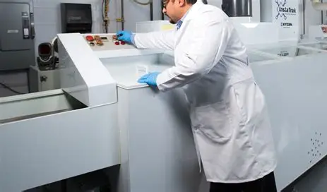
Applying solder mask at home requires attention to surface preparation and curing conditions to achieve consistent results. Poor adhesion or incomplete coverage can lead to peeling during soldering or environmental exposure. Following established practices helps minimize these issues without specialized factory equipment.
Technical Principles Behind DIY Solder Mask Application
Solder mask materials used in home settings are typically UV-curable liquid inks or films. These formulations contain photoinitiators that trigger polymerization when exposed to ultraviolet light of the correct wavelength. The cured polymer bonds to the cleaned copper and laminate surfaces, forming a durable barrier. Adhesion depends on thorough surface cleaning to remove oxides, oils, and etching residues.
Thermal or additional UV post-curing steps further cross-link the polymer, enhancing chemical resistance and mechanical strength. According to IPC-6012 specifications for rigid printed boards, the coating must maintain integrity under expected operating conditions. Hobbyists achieve acceptable results by controlling exposure time, light intensity, and development chemistry to match the mask material properties.
Step-by-Step Process for Applying Red Solder Mask at Home
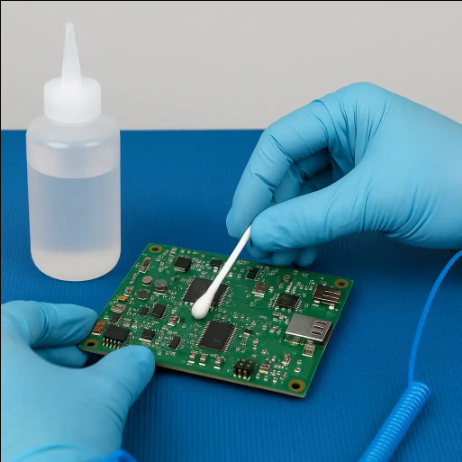
Begin with a thoroughly cleaned and dried PCB. Remove any remaining photoresist or etching byproducts using appropriate solvents followed by rinsing and baking to eliminate moisture. Apply the red solder mask material evenly across the board surface using a brush, roller, or screen-printing technique suited to the chosen product. Ensure the coating thickness remains consistent to avoid thin spots or excessive buildup around fine traces.
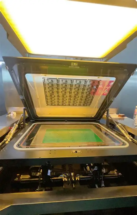
Place a transparency or film mask over the coated board that blocks UV light from the areas where pads and holes must remain exposed. Expose the assembly to a UV source for the duration recommended by the mask supplier. After exposure, develop the board in the specified solution to remove unexposed mask material, revealing the desired openings. Rinse thoroughly and perform a final cure, either by additional UV exposure or controlled heating, to complete the polymerization.
Inspect the finished board under magnification for uniform coverage, proper pad definition, and absence of pinholes or bridging. Touch up any defects with a small brush and repeat the curing step as needed. This methodical approach supports reliable DIY red solder mask application on single- or double-sided boards.
Common Challenges and Practical Solutions
Uneven application often results from inadequate surface preparation or inconsistent coating technique. Repeating the cleaning process and practicing on scrap boards improves coverage. Overexposure or underexposure can cause either incomplete removal of mask or loss of fine features; adjusting exposure time in small increments helps dial in the correct parameters for a given setup.
Peeling or poor adhesion frequently traces back to residual contaminants or moisture. Extended drying after cleaning and ensuring the board reaches room temperature before coating reduce these risks. When working with fine-pitch designs, thinner application layers and precise mask alignment become especially important to maintain pad definition.
Conclusion
Applying red solder mask at home enhances both the functionality and appearance of DIY PCBs when performed with attention to cleaning, exposure control, and curing. The process follows established engineering principles that align with industry expectations for coating performance. Hobbyists who master these steps produce boards better suited for assembly, testing, and extended use in their projects.
FAQs
Q1: How does DIY red solder mask application improve homemade PCB fabrication?
A1: Red solder mask protects copper traces, prevents solder bridging, and provides electrical insulation while offering high visual contrast for easier assembly and inspection. Proper application following basic preparation and curing steps yields boards with improved durability suitable for hobbyist electronics projects.
Q2: What are the key steps to apply solder mask at home successfully?
A2: Successful application involves thorough cleaning of the etched board, even coating of the red mask material, precise UV exposure through a film mask, development to open pads, and final curing. Consistent technique and attention to surface condition help achieve uniform coverage and adhesion on DIY boards.
Q3: Why choose red solder mask for hobbyist projects over other colors?
A3: Red provides excellent contrast against copper and component markings, simplifying visual inspection and documentation. It also maintains the same protective and insulating properties as other colors while adding aesthetic appeal to completed assemblies.
Q4: What common issues arise during homemade PCB solder mask application?
A4: Common issues include uneven coverage, poor adhesion, and incomplete pad definition, often caused by surface contamination, incorrect exposure times, or moisture. Addressing these through repeated cleaning, incremental exposure adjustments, and proper drying improves outcomes in DIY red solder mask application.
References
IPC-A-600K — Acceptability of Printed Boards. IPC, 2020
IPC-6012E — Qualification and Performance Specification for Rigid Printed Boards. IPC, 2017
ISO 9001:2015 — Quality Management Systems. ISO, 2015