ALLPCB


Introduction: Uncovering the Cost Iceberg of Multi-Layer PCBs
In the age of high-density electronics, multi-layer PCBs are the heart of countless cutting-edge devices. From the smartphone in your hand to the servers powering data centers, they all rely on complex, precision-engineered multi-layer PCBs. Compared to single or double-layer boards, multi-layer boards offer higher routing density, superior electrical performance, and better noise immunity, but they also come with more intricate manufacturing processes and higher costs.
For many PCB engineers and purchasers, the cost of a multi-layer board can feel like a 'black box,' full of uncertainty and confusion. Why do different parameter choices lead to vastly different prices for the same design? What are the biggest cost drivers? How can you effectively control costs without compromising product performance?
As a professional PCB manufacturing service provider, ALLPCB understands these pain points. This article will peel back the layers of multi-layer PCB cost composition from a manufacturer's perspective, from design files to final product, revealing the secrets behind the price tag. Our goal is to provide a practical guide that empowers you to make smart, cost-effective decisions at every critical stage of your project—from design to ordering.

10 Layer PCB Stack up
An Overview of Key Cost Elements
Before we dive into the details, let's get a high-level view of the core factors that influence multi-layer PCB costs. Unlike the simple 'material + processing' model of single/double-layer boards, a multi-layer board's cost is a complex system determined by six key dimensions:
- Layer Count: This is the most direct and impactful factor. More layers mean a more complex manufacturing process and higher costs.
- Material Selection: The type and performance of the base material are fundamental cost drivers.
- Size and Shape: These determine the raw material consumption and production efficiency.
- Manufacturing Process Complexity: This is the primary source of cost variance, including trace precision, hole types, and surface finish.
- Order Quantity and Lead Time: Economies of scale and time are crucial in any production process.
- Testing and Quality Requirements: The extra investment required to ensure product reliability.
These six factors are not isolated; they are interconnected and influence each other. A comprehensive understanding of them is essential to proactively manage and optimize multi-layer PCB costs.
In-Depth Analysis: The Key Factors Driving Multi-Layer PCB Costs
3.1 Layer Count: The Foundation of PCB Cost
Layer count is the number one driver of multi-layer board pricing. Every additional layer means increased material usage and, more importantly, a multiplication of manufacturing steps: extra lamination, drilling, plating, etching, and AOI inspection. Each lamination requires precise alignment and high temperature/pressure, and each drilling cycle requires re-calibration. These extra steps not only consume more time and material but also increase the risk of errors, which lowers the yield rate.
Therefore, at the beginning of your design, choose the minimum number of layers that meets your electrical performance requirements (e.g., signal integrity, power integrity, EMI/EMC). Do not add layers unnecessarily for aesthetic reasons.
3.2 Material Selection: The Art of Balancing Performance and Cost
The PCB substrate is the 'skeleton' of a multi-layer board, and its selection directly determines the board's electrical performance and cost.
- Standard FR-4: This is the most common and cost-effective material, offering good electrical properties and mechanical strength. It's suitable for most general-purpose electronics.
- High-Tg Laminates: For high-temperature environments, standard FR-4 may not be sufficient. High-Tg (high glass transition temperature) materials provide better heat resistance and are slightly more expensive.
- High-Speed/Low-Loss Laminates: For high-speed digital signals like USB 3.0, PCIe, or DDR, you need special laminates with a lower dissipation factor (Df). These materials use specialized resins and glass fibers and can be several times more expensive than FR-4.
- High-Frequency Laminates: Used for RF, microwave, and millimeter-wave applications. Materials like Rogers or Isola have strictly controlled dielectric constants (Dk) and dissipation factors (Df), ensuring stable signal transmission. They are the most expensive option.

Comparing Different Board Materials
3.3 Size and Panel Utilization: Optimizing Every Square Inch
The final cost of a PCB is directly tied to its physical size and shape.
- Individual Board Size: A larger board consumes more raw material, which is obvious.
- Panelization: Factories produce PCBs on large panels. By combining multiple smaller boards onto a single large panel (a process called panelization), they increase efficiency and spread fixed costs. Therefore, if your PCB design fits standard panel sizes efficiently, you'll benefit from a lower bulk PCB price.
- Irregular Shapes: Unlike simple rectangular boards, irregularly shaped PCBs require extra CNC routing and may need custom tooling, which incurs additional PCB fabrication costs.

Panelization Efficiency: Lower vs Higher
3.4 Manufacturing Process Complexity: The Real Cost Driver
This is the most intricate aspect of multi-layer PCB costs. Every seemingly minor parameter choice can lead to a significant price difference.
- Trace Design Precision (Trace/Space): Standard trace width and spacing (e.g., 6/6 mil or 5/5 mil) require common equipment, have a high yield rate, and are low-cost. However, when you opt for finer lines (e.g., 4/4 mil or 3/3 mil) for high-density routing, you need more expensive exposure equipment and precision etching processes. This drastically increases the manufacturing difficulty and lowers the yield, pushing up your costs.
- Hole Type and Size:
- Through-hole Vias: These are the most common type, drilled straight through all layers. The process is mature and the cost is the lowest.
- Blind Vias and Buried Vias: These are used for high-density interconnect (HDI) boards to save space. However, they require sequential drilling, multiple lamination, and plating steps, making them far more complex and costly than through-hole vias.
- Hole Size: The smaller the hole, the more fragile the drill bit and the higher the risk of breakage, requiring more frequent bit changes. This increases production time and lowers the yield, directly raising both PCB prototype costs and bulk prices.
- Surface Finish:
- HASL (Hot Air Solder Leveling): The most cost-effective option, offering good solderability but a slightly uneven surface. It's not ideal for fine-pitch components like BGAs.
- ENIG (Electroless Nickel Immersion Gold): Offers excellent planarity, solderability, and a long shelf life, making it a popular choice for BGA and other precision packages. However, its cost is significantly higher than HASL.
- OSP (Organic Solderability Preservative): An eco-friendly and low-cost option, but with a short shelf life.

Comparing Different Surface Finishes
- Special Processes:
- Back-drilling: Used for high-speed signals to remove 'stubs' in through-holes, reducing signal reflection. It adds a precision drilling step.
- Via-in-pad: Placing a via directly on a component pad, which requires resin filling and surface plating, is a complex process that adds significant cost.

Various Types of Holes Affect Costs
3.5 Order Quantity and Lead Time: Economies of Scale and Time
- Order Quantity: PCB production involves fixed costs like setup fees and tooling. For a small prototype run, these costs are spread over only a few boards, resulting in a high per-unit price. By contrast, a large-volume order benefits from economies of scale, significantly lowering the unit cost.
- Lead Time: If your project timeline is flexible, a standard lead time (e.g., ALLPCB's 5-7 days) is the most cost-effective option. For an urgent order, you'll need to pay a premium because the factory must prioritize your job, which may require overtime or disrupting the normal production schedule.
From Order to Production: How ALLPCB Helps You Optimize Costs
Now that you understand the cost drivers, let's explore how to control them. At ALLPCB, we leverage technology and streamlined processes to provide a transparent, efficient, and highly competitive multi-layer PCB purchasing experience.
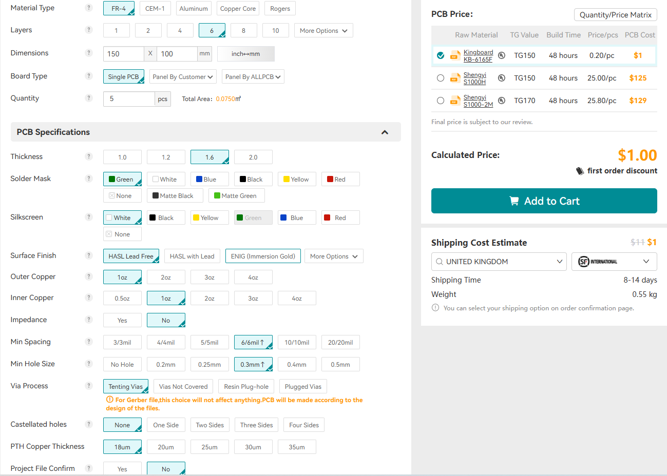
- Intelligent Online Quotation System: Our system eliminates the hassle and uncertainty of traditional quotes. By simply entering your parameters on the ALLPCB quotation page, you receive an instant, accurate quote. You can immediately see how each parameter (e.g., layer count, material, hole size, surface finish) impacts the price, empowering you to make the most cost-effective decisions before you even place your order.

PCB Online Quoting of ALLPCB
- Professional DFM Analysis: After you submit your files, our team of experienced engineers performs a free DFM (Design for Manufacturability) analysis. We proactively identify potential manufacturing risks and design flaws—such as insufficient trace-to-trace spacing or improper via design—and provide recommendations. This not only prevents rework and delays but also significantly improves the final product's yield rate, saving you money from the very beginning.

ALLPCB DFM Checking
- Efficient Supply Chain Integration: ALLPCB integrates a vast network of high-quality PCB manufacturers worldwide. This allows us to secure lower raw material costs and intelligently match your order with the most suitable factory, ensuring you receive a competitive PCB manufacturing cost without sacrificing quality.
Cost Optimization Guide: Practical Advice for Engineers and Purchasers
1. Cost Control at the Design Stage
- Be Precise: Accurately assess your electrical and mechanical performance needs. Avoid using high-performance, high-cost solutions if they aren't necessary.
- Simplify Layers: Choose the minimum number of layers that meets your signal integrity requirements.
- Simplify Manufacturing: Use through-hole vias whenever possible, and avoid blind and buried vias unless they are essential. Loosen trace/space and hole size parameters if you can.
2. Cost Control at the Ordering Stage
- Use the Intelligent Quoting Tool: Experiment with different parameter combinations on the ALLPCB quotation page to find the most cost-effective solution that fits your budget and performance needs.
- Plan Ahead: If your project has a future production run, consider combining prototyping with a small-batch run to take advantage of ALLPCB's bulk discounts.
- Choose Standard Lead Times: Place your order in advance to avoid expensive expedited fees.
3. Standardize Your Files
- Submitting clear, accurate Gerber files and a standardized readme document significantly reduces communication overhead and prevents production delays caused by file issues.
Conclusion: Master Your Costs, Master Your Success
The multi-layer PCB cost composition is a complex system, but by understanding its core drivers, you can proactively control your expenses. Through intelligent design decisions and a smart purchasing strategy, you can get the high-quality PCBs you need without breaking the bank.
ALLPCB is committed to providing a transparent, efficient, and cost-effective PCB manufacturing platform for engineers and purchasers worldwide. We believe that with our intelligent tools and professional services, you'll be empowered to make the best purchasing decisions and gain a competitive edge in the market.
Take control of your PCB costs today! Visit the ALLPCB quotation page to experience transparent, smart multi-layer PCB online quoting and begin your journey to cost optimization!