 ALLPCB


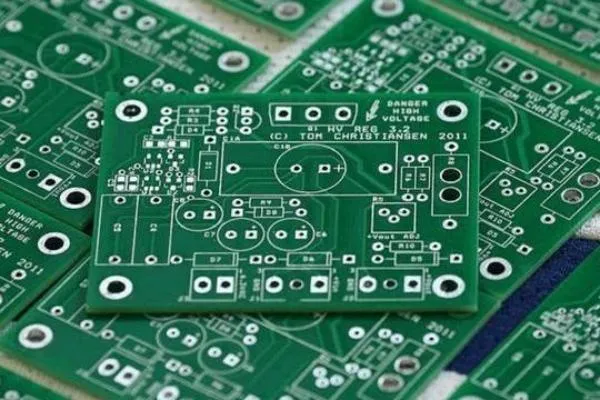
If you're looking for a clear and detailed explanation of solder mask application on single-sided PCBs, you've come to the right place. In simple terms, a solder mask is a protective layer applied to a printed circuit board (PCB) to shield copper traces from oxidation, prevent solder bridges during assembly, and enhance the board's lifespan. For single-sided PCBs, where components are mounted on just one side, the solder mask application process is critical to ensuring functionality and durability. This guide dives deep into the process, techniques, and best practices for applying solder mask on single-sided PCBs, helping you understand its role in the manufacturing process and PCB protection.
Whether you're an engineer, designer, or hobbyist, this blog will walk you through everything you need to know about PCB solder mask application in single-sided PCB manufacturing. From the basics of what a solder mask is to step-by-step application methods, we’ve got you covered with practical insights and tips for achieving optimal results.
What is a Solder Mask and Why is it Important for Single-Sided PCBs?
A solder mask, often called solder resist, is a thin polymer layer applied to the surface of a PCB. Its primary role is to protect the copper traces on the board from environmental factors like dust, moisture, and oxidation, which can degrade conductivity over time. On a single-sided PCB, where all components and traces are on one side of the board, the solder mask also prevents accidental solder bridges during the assembly process, ensuring that solder only adheres to the designated pads.
The importance of a solder mask in single-sided PCB manufacturing cannot be overstated. Without this protective layer, the exposed copper would be vulnerable to corrosion, leading to potential short circuits or complete board failure. Additionally, the solder mask provides insulation, reducing the risk of electrical interference between closely spaced traces. For a typical single-sided PCB used in simple electronics like calculators or LED circuits, a well-applied solder mask can extend the board's operational life by years, even in harsh conditions.
Understanding Single-Sided PCB Manufacturing
Before diving into the specifics of solder mask application, it’s helpful to understand the broader single-sided PCB manufacturing process. Single-sided PCBs are the simplest type of circuit boards, with copper traces and components on just one side of a non-conductive substrate, often made of materials like FR-4 (a fiberglass epoxy laminate). These boards are commonly used in low-cost, low-complexity applications due to their simplicity and affordability.
The manufacturing process for single-sided PCBs typically follows these steps:
- Design and Layout: The circuit design is created using software, defining the placement of traces and components on one side of the board.
- Substrate Preparation: A base material, such as FR-4, is cut to size and cleaned to remove contaminants.
- Copper Cladding: A thin layer of copper is laminated onto one side of the substrate.
- Etching: Unwanted copper is removed through a chemical process, leaving only the desired circuit traces.
- Drilling: Holes are drilled for through-hole components or mounting purposes.
- Solder Mask Application: A protective layer is applied to cover the copper traces, leaving only the solder pads exposed.
- Silkscreen Printing: Labels and markings are added for component placement and identification.
- Final Inspection: The board is tested for defects before assembly.
Among these steps, solder mask application plays a pivotal role in ensuring the board’s reliability. Let’s explore this process in detail.
Types of Solder Masks Used in Single-Sided PCB Manufacturing
There are several types of solder masks available, each with unique properties suited for different applications. Understanding these options can help in selecting the right one for your single-sided PCB project.
- Liquid Photoimageable Solder Mask (LPI): This is the most common type used today due to its precision. LPI is applied as a liquid, then exposed to UV light through a photomask to define areas that need protection. It’s ideal for single-sided PCBs with complex trace patterns, offering excellent adhesion even on uneven surfaces.
- Dry Film Solder Mask (DFSM): This type comes as a solid film that is laminated onto the PCB surface under heat and pressure. While it provides uniform thickness, it’s less adaptable to intricate designs compared to LPI and is often used for simpler single-sided boards.
- Epoxy Liquid Solder Mask: Applied via silkscreen printing, this older method is less precise but cost-effective for basic single-sided PCBs. It’s cured thermally and suits low-budget projects where high precision isn’t critical.
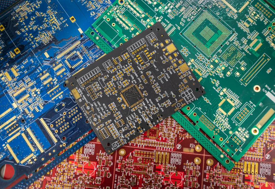
For most modern single-sided PCB designs, LPI is preferred due to its balance of cost, precision, and durability. The choice of solder mask also influences the board’s final color—green is the standard, but options like red, blue, black, and white are available for aesthetic or functional purposes.
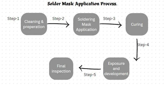
Step-by-Step Guide to Solder Mask Application on Single-Sided PCBs
Applying a solder mask to a single-sided PCB requires precision to ensure complete coverage and protection. Below is a detailed breakdown of the process, focusing on the widely used Liquid Photoimageable Solder Mask (LPI) method.
Step 1: Surface Preparation
Before applying the solder mask, the PCB surface must be thoroughly cleaned to remove any dust, grease, or oxidation from the copper traces. This is typically done using a chemical cleaner or micro-etching process to ensure proper adhesion of the mask. A clean surface is critical—any contaminants can cause the solder mask to peel or bubble, compromising PCB protection.
Step 2: Application of Solder Mask
For LPI, the liquid solder mask is applied to the single side of the PCB using techniques like spray coating or curtain coating. Spray coating is common for small batches, ensuring an even layer of approximately 0.8 to 1.2 mils (20-30 micrometers) thick. The goal is to cover all copper traces while leaving solder pads exposed for component attachment.
Step 3: Pre-Curing (Tack Drying)
After application, the board undergoes a pre-curing process at a low temperature (around 70-80°C) for 10-20 minutes. This step partially hardens the solder mask, making it tacky but not fully cured, preparing it for the next stage of pattern definition.
Step 4: Exposure to UV Light
A photomask, which is a film with the desired pattern, is placed over the PCB. The board is then exposed to UV light, typically at a wavelength of 365 nm, for a few seconds. The UV light hardens the solder mask in areas not covered by the photomask, defining where the mask will remain after development.
Step 5: Development
The PCB is immersed in a developer solution, usually a mild alkaline liquid, to remove the unexposed solder mask material. This reveals the solder pads and other areas meant for soldering, while the rest of the board remains covered by the hardened mask.
Step 6: Final Curing
The board is then subjected to a final thermal curing process at a higher temperature (around 150°C) for about 30-60 minutes. This fully hardens the solder mask, enhancing its durability and resistance to heat, chemicals, and mechanical stress during assembly and operation.
Step 7: Inspection
Finally, the PCB is inspected for defects like pinholes, uneven coverage, or misalignment of the solder mask. Advanced manufacturers often use Automated Optical Inspection (AOI) systems to ensure quality, checking for coverage accuracy down to 0.1 mm tolerances.
Best Practices for Effective Solder Mask Application
To achieve optimal results during solder mask application in single-sided PCB manufacturing, consider these best practices:
- Ensure Design Accuracy: Include a dedicated solder mask layer in your PCB design files (often in Gerber format). Define clearances around pads—typically 2-4 mils (0.05-0.1 mm) larger than the pad size—to prevent mask overlap during application.
- Choose the Right Material: Select a solder mask type based on your board’s complexity and budget. For intricate designs, LPI offers better precision; for basic boards, epoxy might suffice.
- Maintain Cleanliness: Any residue on the PCB can lead to adhesion issues. Use proper cleaning protocols before application to avoid defects.
- Control Thickness: Aim for a consistent solder mask thickness of 0.8-1.2 mils to balance protection and manufacturability. Too thick a layer can cause issues during soldering, while too thin a layer may not provide adequate protection.
- Test for Compatibility: Ensure the solder mask material is compatible with the soldering process (e.g., reflow soldering temperatures up to 260°C) to prevent cracking or discoloration.
Common Challenges in Solder Mask Application and Solutions
Even with careful planning, issues can arise during solder mask application. Here are some common challenges specific to single-sided PCBs and how to address them:
- Uneven Coverage: This can occur due to improper application techniques or surface contaminants. Solution: Use automated coating equipment for consistency and ensure thorough cleaning beforehand.
- Pinholes or Voids: Small holes in the solder mask can expose copper, leading to oxidation. Solution: Adjust the viscosity of the liquid mask and optimize curing conditions to prevent air bubbles.
- Misalignment: If the solder mask doesn’t align with pads, it can cover areas meant for soldering. Solution: Use high-precision photomasks and double-check design files for accuracy.
- Peeling or Delamination: Poor adhesion can cause the mask to peel off over time. Solution: Enhance surface preparation and choose a mask material with strong bonding properties for the substrate used.
Benefits of Proper Solder Mask Application in PCB Protection
A well-applied solder mask offers numerous benefits, especially for single-sided PCBs used in various applications. Here’s why investing in quality solder mask application pays off:
- Enhanced Durability: Protects copper traces from oxidation and environmental damage, extending the board’s lifespan by up to 10-15 years in typical conditions.
- Improved Reliability: Prevents solder bridges, reducing the risk of short circuits during assembly—a critical factor for boards with trace spacing as tight as 6 mils (0.15 mm).
- Cost Savings: Minimizes rework and failures, saving on repair and replacement costs over time.
- Aesthetic Appeal: Provides a polished, professional look to the PCB, which can be important for consumer-facing products.
Conclusion: Mastering Solder Mask Application for Single-Sided PCBs
Applying a solder mask to a single-sided PCB is a crucial step in the PCB manufacturing process, ensuring both protection and functionality. By understanding the types of solder masks, following a meticulous application process, and adhering to best practices, you can achieve a high-quality result that enhances PCB protection and reliability. Whether you’re working on a simple project or a larger production run, paying attention to details like surface preparation, mask thickness, and curing conditions can make all the difference.
At ALLPCB, we’re committed to supporting your journey through every stage of PCB manufacturing. With the insights from this guide, you’re well-equipped to tackle solder mask application for single-sided PCBs, ensuring your designs are both durable and efficient. Keep these tips in mind for your next project, and you’ll be on your way to creating robust, long-lasting circuit boards.


