 ALLPCB


Introduction
Ceramic printed circuit boards represent a critical advancement in electronics for applications demanding superior thermal management, mechanical stability, and electrical performance. Unlike traditional organic substrates, ceramic PCBs excel in high-power density environments such as power electronics, aerospace systems, and RF modules, where heat dissipation and reliability under extreme conditions are paramount. This guide delves into three primary ceramic PCB manufacturing processes: High Temperature Co-fired Ceramic (HTCC), Low Temperature Co-fired Ceramic (LTCC), and Thick Film printing. Each method offers distinct advantages in ceramic PCB manufacturing, tailored to specific engineering requirements like multilayer integration or cost efficiency.
Understanding these ceramic PCB processes is essential for electrical engineers designing boards that must withstand elevated temperatures, thermal cycling, and harsh operational stresses. HTCC provides robust, hermetic structures ideal for military and space applications, while LTCC enables embedding of passives for compact RF designs. Thick film processes deliver economical solutions for hybrid circuits and sensors. By examining the step-by-step workflows, comparisons, and best practices, engineers can select the optimal ceramic PCB process to meet performance targets without compromising yield or reliability.
Why Ceramic PCBs Matter for Electrical Engineers
Ceramic PCBs address key limitations of FR-4 and other organic laminates, particularly in scenarios involving high thermal loads and coefficient of thermal expansion (CTE) mismatches with silicon dies. Materials like alumina or aluminum nitride provide thermal conductivities far exceeding standard PCBs, enabling efficient heat spreading in power converters and LED drivers. This inherent stability reduces warpage and delamination risks during assembly and operation, critical for long-term reliability in automotive and industrial controls.
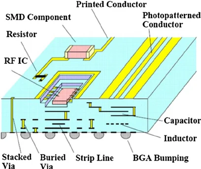
The relevance of ceramic PCB manufacturing extends to miniaturization trends, where integrating resistors, capacitors, and inductors directly into the substrate minimizes parasitics and board space. Engineers benefit from ceramics' low dielectric loss at high frequencies, making them suitable for microwave circuits and 5G infrastructure. Moreover, their resistance to chemicals and radiation suits harsh environments, aligning with demands in defense and medical imaging. Selecting the right ceramic PCB process ensures compliance with performance specs while optimizing manufacturability.
Factory-driven insights reveal that ceramic substrates enable direct bonding or printing of conductors without adhesives, enhancing interfacial strength. This direct integration supports higher current densities and voltage ratings compared to metal-clad PCBs. For electrical engineers, grasping these processes informs design rules, such as via placement and layer count, to avoid common pitfalls like shrinkage-induced misalignment.
HTCC Ceramic PCB Manufacturing Process
The HTCC ceramic PCB process begins with the preparation of green ceramic tapes, typically composed of alumina or aluminum nitride powders mixed with binders and plasticizers. These tapes are cast to precise thicknesses, dried, and cut into sheets matching the final board outline. Mechanical punching creates vias for interlayer connections, followed by filling with refractory metal pastes like tungsten or molybdenum, which withstand subsequent high-temperature steps.
Screen printing applies conductor, dielectric, and via-fill pastes onto individual layers using fine-mesh stencils for pattern definition. Multiple prints build up thickness where needed, and layers are then stacked in precise alignment using optical fiducials. Isostatic lamination under pressure and heat bonds the stack into a flexible green laminate, preparing it for sintering.
The core of HTCC lies in co-firing: the entire laminate undergoes binder burnout at intermediate temperatures to remove organics without cracking, followed by high-temperature sintering above 1500°C in a controlled atmosphere. This densifies the ceramic matrix and metallizes conductors simultaneously, achieving hermetic seals and high mechanical integrity. Post-firing, external terminations are added via plating or brazing, and final machining contours the board.
This process yields multilayer HTCC ceramic PCBs with excellent thermal matching to semiconductors, but demands precise control over shrinkage, typically 15-20% uniformly across layers. Engineers must account for this in design files to ensure via registration post-sintering.
LTCC Ceramic PCB Manufacturing Process
LTCC ceramic PCB manufacturing starts similarly with green tape casting, but uses glass-ceramic compositions that soften at lower temperatures, incorporating fillers for tailored dielectric properties. Tapes are punched for vias and cavities, enabling embedded components like capacitors during stacking. Conductive pastes, often silver or copper-based, fill vias and print circuits on each layer via screen printing.
After printing and drying individual layers, they are collated, aligned, and laminated under uniaxial or isostatic pressure to form a cohesive tape stack. This green assembly undergoes low-temperature co-firing around 850-900°C, where the glass phase flows to densify the structure while sintering metals without oxidation, thanks to inert atmospheres.
Post-firing polishing and metallization complete the LTCC ceramic PCB, with options for surface passivation or resistor trimming. The process excels in integrating passives, as dielectric layers can form capacitors in-situ, reducing discrete component count. Shrinkage control is finer than HTCC due to lower viscosities, aiding high-density interconnects.
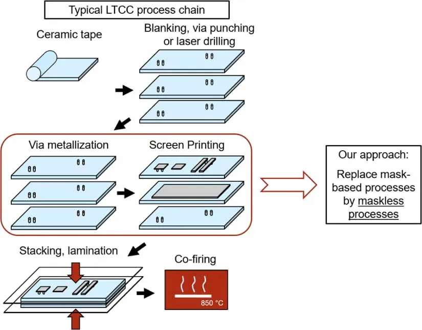
Factory practices emphasize tape quality to minimize defects like pinholes in fired conductors. This makes LTCC ideal for RF modules where low-loss transmission lines are critical.
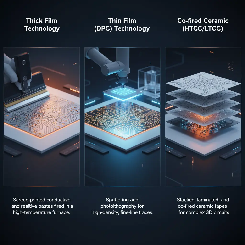
Thick Film Ceramic PCB Manufacturing Process
Thick film ceramic PCB production commences with substrate selection, usually 96% alumina for its balance of cost and properties, cleaned to remove contaminants. Screen printing deposits conductor pastes (palladium-silver or platinum-gold), dielectric overglazes, or resistor formulations through emulsions onto the surface.
Each printed layer undergoes drying to evaporate solvents, followed by firing in a belt furnace at 800-900°C, where organic binders burn off and particles sinter into dense films tens of microns thick. Multiple sequential print-dry-fire cycles build multilayers, with dielectrics isolating conductor runs.
Resistors receive laser trimming for precision values, and terminations are fired or plated for solderability. Unlike co-fired methods, thick film avoids full laminate sintering, allowing hybrid assembly with wire bonding or flip-chip later.
This iterative approach suits prototyping and low-to-medium volumes, offering flexibility for custom hybrids without high tooling costs.
Comparing HTCC, LTCC, and Thick Film Ceramic PCBs
HTCC ceramic PCBs prioritize ultimate reliability through high-density sintering, supporting complex 3D structures but at higher costs and longer lead times due to refractory materials and elevated temperatures. LTCC offers a cost-performance sweet spot with noble metal conductors and embedded passives, favored for RF and telecom where multilayer flexibility shines. Thick film provides the simplest, most economical path for single- or few-layer boards, excelling in sensors and power hybrids with rapid iteration.
Key differentiators include firing temperatures: HTCC exceeds 1500°C, LTCC 850-950°C, and thick film per-layer below 900°C, impacting material choices and integration. Multilayer capability peaks in co-fired processes (up to 50+ layers), while thick film limits to 10-20 via overprinting. Thermal performance is strong across all, but HTCC edges in hermeticity for vacuum apps.
- Firing Temperature: HTCC >1500°C; LTCC 850-950°C; Thick Film 800-900°C per layer
- Conductor Metals: HTCC W/Mo; LTCC Ag/Au/Cu; Thick Film Pd-Ag/Pt-Au
- Layer Capability: HTCC high (20-100+); LTCC high (10-50+); Thick Film low-medium (1-20)
- Cost: HTCC high; LTCC medium; Thick Film low
- Best For: HTCC hermetic, high-power; LTCC RF, embedded passives; Thick Film hybrids, sensors
Engineers select based on volume, frequency needs, and integration density.
Best Practices and Quality Control in Ceramic PCB Manufacturing
Adhering to standardized inspection protocols ensures ceramic PCB process integrity from tape casting to final test. Visual and dimensional checks post-lamination detect warpage or misalignment early, using IPC-A-600 criteria for acceptability of printed boards. Automated optical inspection verifies print registration, while X-ray scans confirm via fills.
During firing, controlled ramps prevent cracks from thermal gradients, with post-sinter metrology quantifying shrinkage uniformity. Electrical testing includes insulation resistance and continuity, per qualification specs like IPC-6012. Quality management systems aligned with ISO 9001:2015 maintain traceability and process controls.
Best practices include design for uniform shrinkage via symmetric patterns and fiducial arrays. Substrate handling minimizes contamination, and paste viscosity control optimizes rheology for defect-free prints.
Conclusion
Mastering HTCC, LTCC, and thick film ceramic PCB manufacturing empowers electrical engineers to tackle demanding applications with precision. HTCC delivers unmatched durability, LTCC versatility for integration, and thick film accessible performance. By aligning process choice with design goals and enforcing rigorous quality measures, teams achieve reliable, high-yield production. These ceramic PCB processes continue evolving to support next-generation electronics.
FAQs
Q1: What are the key steps in HTCC ceramic PCB manufacturing?
A1: HTCC ceramic PCB manufacturing involves green tape preparation, via punching and filling, screen printing of circuits, layer stacking and lamination, and high-temperature co-firing above 1500°C. Binder burnout precedes densification to form hermetic multilayers. This process suits high-reliability needs but requires shrinkage compensation in designs. Factory controls ensure via alignment post-sintering.
Q2: How does LTCC ceramic PCB process differ from thick film?
A2: LTCC ceramic PCB process uses tape stacking and low-temperature co-firing for multilayers with embedded passives, while thick film applies sequential print-fire cycles on rigid substrates without full co-firing. LTCC enables higher layer counts and RF performance, whereas thick film offers faster prototyping. Both leverage screen printing but diverge in complexity and cost.
Q3: What advantages does thick film ceramic PCB offer in manufacturing?
A3: Thick film ceramic PCB manufacturing provides low-cost, flexible production via iterative printing and firing on alumina substrates, ideal for hybrids and sensors. It avoids co-firing challenges, allowing easy resistor integration and trimming. This ceramic PCB process supports quick design changes without new tooling.
Q4: Why reference standards like IPC in ceramic PCB quality control?
A4: Standards such as IPC-A-600 guide acceptability criteria for ceramic PCB manufacturing, covering visuals, dimensions, and defects. They standardize inspections across processes like HTCC and LTCC, ensuring consistency. ISO 9001 supports overall process reliability.
References
IPC-A-600K — Acceptability of Printed Boards. IPC, 2020
IPC-6012E — Qualification and Performance Specification for Rigid Printed Boards. IPC, 2017
ISO 9001:2015 — Quality Management Systems. ISO, 2015


