ALLPCB


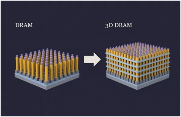
What is a channel hole?
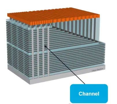
A channel hole is a slender, vertical hole that extends from the top to the bottom of the wafer surface, passing through multiple layers of memory cells. These holes penetrate the entire stacked structure and are filled with conductive material to form conductive channels between each memory layer, allowing electrons to move between storage cells for read, write, and erase operations. The hole depth depends on the number of control gate layers; for stacks exceeding 400 layers the depth is around 10 micrometers, while the hole diameter is typically about 100 nm, so channel hole etching is a high aspect ratio etch.
Channel hole etching process steps
Etching is carried out in three main steps: deposition of an amorphous carbon film, etching of the carbon film, and etching of the channel holes. An amorphous carbon film is deposited because carbon has high etch resistance. During etching of high aspect ratio holes, the carbon mask resists the reactive gases and protects the underlying stack from undesired etching.
Amorphous carbon etch
This step uses IC P-RIE for etching, with O2 as the primary etch gas.

Channel hole etch
The channel holes are etched using CCP-RIE, with fluorine-containing gases as the main etchants.

Key considerations for channel hole etching
- Hole diameter uniformity: Maintain consistent diameters across all holes to prevent variability in storage performance.
- Sidewall smoothness: Sidewall roughness affects the quality of subsequent material fill.
- Etch depth control: Ensure each hole reaches the same depth to guarantee uniform and reliable storage layers.
- Mask erosion: Use a hard mask with sufficient durability to avoid erosion during prolonged etching.
- Feature distortion: Prevent bending, twisting, or tilting of holes caused by stress.

Cleaning and residue removal: During etching, etch products at the bottom of the holes must be removed promptly to avoid contamination or defects.