ALLPCB


Overview
Memory bandwidth has become an increasing bottleneck in AI servers, limiting system compute efficiency. HBM has gained traction because it offers higher data transfer rates than conventional DRAM, but HBM bandwidth will also face limits as AI workloads evolve. In theory, compute-in-memory could fully address the "memory wall," but commercial maturity and mass production of such solutions remain distant. In this context, 3D DRAM is emerging as a promising alternative to HBM.
Industry Progress
Major memory vendors and semiconductor research organizations worldwide are developing 3D DRAM and have made significant progress toward mass-production-ready products.
According to industry sources in the Seoul semiconductor sector, Samsung disclosed its 3D DRAM development roadmap at the Memcon 2024 chip manufacturing summit in San Jose, California.
In early April, Samsung said it plans to introduce an early version of 3D DRAM based on vertical channel transistor technology in 2025. This approach orients a channel vertically within the transistor cell and surrounds it with a gate to act as a switch. The company also plans to deliver an updated stacked DRAM by 2030 that can stack all cell elements, including capacitors.
Why Move Beyond Planar DRAM
AI workloads continuously raise demands on memory speed and density. Against rapidly growing data volumes and increasing processor compute, planar (2D) DRAM is becoming constrained in both density and speed. Current DRAM process technology is approaching its limits (the most advanced DRAM processes are around 12 nm), and further scaling is increasingly difficult because of DRAM cell architecture: each storage cell consists of a transistor and a capacitor, and process scaling in a single plane faces two major challenges: first, scaling the capacitor; second, charge sharing from the capacitor to the digitline, which depends on transfer time and digitline length. The required depth-to-width ratio of storage capacitors increases dramatically with process shrink, making planar DRAM scaling progressively harder.
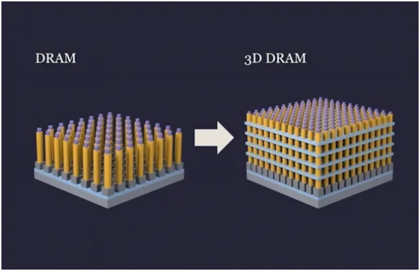
Consequently, designers are considering 3D architectures similar to 3D NAND. 3D DRAM stacks storage cells above logic to increase capacity per unit area and address the deep-and-narrow capacitor challenge of planar DRAM. 3D stacking can also enable reuse of storage capacitors across layers, potentially reducing cost per bit. The multi-layer transistor stacking in 3D DRAM can increase spacing between transistors and reduce leakage current.
In short, 3D DRAM stacks storage cells vertically rather than laying them out horizontally, increasing capacity per unit area by multiple times. For example, a notional 3D DRAM basic capacity could be around 100 GB versus current upper-end DRAM capacities near 36 GB.
Related Reading: Understanding Why DRAM Requires Refreshing
Development Paths for 3D DRAM
There are two main development paths for 3D DRAM. The most direct approach preserves current DRAM technology and stacks multiple dies on top of each other. This high-end packaging method is used for HBM; common HBM stacks are 4- and 8-high and could soon reach 16-high. Compared with planar DRAM, die stacking in the package is more expensive because of advanced packaging requirements, but it is justified for bandwidth-hungry applications such as AI.
The other path, and the eventual goal for many vendors, is monolithic stacking. This requires relatively few additional process steps but introduces substantial technical challenges. Some analysts propose that 3D DRAM could emulate 3D NAND by flipping the storage cell orientation. DRAM cells have a small 2D footprint but large vertical capacitors that are tall and hard to layer. As planar dimensions shrink and capacitors become thinner, they must be elongated to retain sufficient charge.
Capacitor Challenges and Capacitor-Free DRAM
Conventional DRAM manufacturing uses circuitry and memory cells on the same plane, with performance improvements historically achieved by shrinking cell size or spacing. Physical limits have been reached: if capacitors become too thin, device reliability is at risk. If the capacitor issue cannot be solved, DRAM storage density and bandwidth will be difficult to improve substantially. To address this, the industry has proposed capacitor-free DRAM combined with 3D stacking as a potential breakthrough.
Capacitor-free DRAM stores information using a single transistor per cell and relies on floating body effects in asymmetric dual-gate polysilicon oxide-semiconductor FETs (a type of multi-gate device) to hold charge without an external capacitor.
Several research organizations are investigating capacitor-free 3D DRAM concepts, including Dynamic Flash Memory, VLT, Z-RAM, and IGZO-FET approaches. To date, the three major memory vendors (Samsung Electronics, SK Hynix, and Micron) have not published extensive details on capacitor-free 3D DRAM implementations.
Performance Benefits
Traditional DRAM requires complex read/write sequences. 3D DRAM can exploit vertically stacked storage cells to access and write data more directly, improving access speed. Advantages of 3D DRAM include high capacity, fast data access, lower power consumption, and improved reliability, making it suitable for a range of applications.
Some market forecasts project the global 3D DRAM market could reach around $100 billion by 2030.
Vendor Efforts and Roadmaps
Recognizing this potential, major memory vendors have intensified R&D efforts.
Samsung has been particularly active. Since 2019 the company has conducted 3D DRAM research and in October 2019 announced an industry-first 12-layer 3D-TSV (Through-Silicon Via) technology. In 2021 Samsung publicly launched its 3D DRAM development project and established a next-generation process development team within its Device Solutions division, led by the company's semiconductor CTO.
At the 2022 SAFE forum, Samsung outlined a logic-stacked chip design called SAINT-D to address DRAM stacking, intended to integrate eight HBM3 chips. Sources report that in May 2023 Samsung formed a team at its semiconductor research center to develop large-scale production of 4F2 cell-structure DRAM. Since DRAM cell size has reached limits, Samsung aims to apply 4F2 to 10 nm-class or more advanced DRAM processes. Successful 4F2 development could reduce die area by about 30% compared with existing 6F2 cells without changing overall process technology.
In October 2023, Samsung announced plans to introduce a new 3D cell structure in next-generation 10 nm-class DRAM rather than a traditional 2D layout. At the 2023 VLSI Symposium in Japan, Samsung presented a paper with 3D DRAM research results and internal chip images. Reports also indicate Samsung has opened a new R&D lab in Silicon Valley focused on 3D DRAM under its Device Solutions America organization. Samsung aims for 2025 production and plans to scale the process node to 8–9 nm by 2027–2028; current leading DRAM processes are around 12 nm.
SK Hynix and Micron
SK Hynix and Micron have not published detailed roadmaps. SK Hynix has discussed its 3D DRAM vision at industry events. According to reports, Cha Seon-yong, vice president responsible for future technology research at SK Hynix, indicated the company would disclose electrical characteristics of its 3D DRAM in 2024 to clarify its development direction. SK Hynix is also exploring IGZO channel materials for future DRAM to improve retention and refresh characteristics; IGZO TFTs have been used in display panels due to moderate carrier mobility, extremely low leakage, and scalability, making IGZO a candidate channel material for stackable DRAM.
Micron began 3D DRAM research as early as 2019. TechInsights statistics showed that by August 2022 Micron had been granted over 30 patents related to 3D DRAM, compared with about 15 for Samsung and about 10 for SK Hynix, indicating Micron holds 2–3 times more 3D DRAM-related patents than the two Korean vendors.
Startups and Processor Industry Interest
Startups are also active. For example, NEO Semiconductor has proposed a 3D X-DRAM technology to overcome DRAM capacity limits. Its cell array layout is similar to 3D NAND and uses FBC techniques to form vertical structures via added layer masks, aiming for high yield, lower cost, and significant density gains. NEO claims 3D X-DRAM can reach 128 Gb density across 230 layers, eight times current DRAM density, with long-term targets of an eightfold capacity increase per decade and 1 Tb cells between 2030 and 2035.
Because memory is tightly coupled with processors, CPU and accelerator vendors are also following 3D DRAM developments. AMD has explored stacking DRAM on compute chiplets following chiplet commercialization, and at ISSCC 2023 presented a multi-layer stacked DRAM vision for servers and HPC accelerators as a likely future direction for HPC memory.
Other processor companies have shown interest as well. For example, Huawei presented a 3D DRAM paper at VLSI Symposium 2022 describing a vertical CAA-type IGZO FET approach, which could accelerate IGZO transistor use in high-density DRAM.
In addition to companies, many global semiconductor research institutions, including research institutes in China, are conducting 3D DRAM research.
Related Reading: DRAM Test and Inspection Design Strategies
Applications and Market Outlook
AI is permeating industries from data centers and cloud servers to smartphones. Devices without AI capabilities will face competitive disadvantages. AI places increasing demands on processors and memory. For small systems such as phones, LPDDR remains adequate for now but may be phased out over time. For large systems, HBM is gaining traction, but its density and bandwidth will eventually become limiting factors. At that point, 3D DRAM could offer a better solution.
In the long term, the automotive sector could adopt 3D DRAM because electric and autonomous vehicles require real-time processing of large data streams from sensors. If processor performance improves while DRAM cannot meet density and bandwidth needs, system-level performance and user experience will suffer. Ensuring DRAM does not become a bottleneck is essential for advanced automotive systems.
Given multiple growing application markets, 3D DRAM has substantial growth potential.