 My Message
 Suggestions


This is the continuation of a series where I create a PCB in every software suite imaginable. Last week, I took a look at KiCad, made the schematic representation for a component, and made a schematic for the standard reference PCB I’ve been using for these tutorials. Now it’s time to take that schematic, assign footprints to parts, and design a circuit board.

The completed schematic for our board
All PCB design tools have different methods of associating the schematic view of a component with how it will be represented on the finished board. Eagle uses libraries that contain both a schematic view and PCB view of a component. In the prehistory of PCB design software, Autotrax simply ignored the schematic view.

Click this button to run PCBnew
KiCad has a clear separation between a symbol (the schematic view) and a footprint (the PCB view). If we were to take our schematic and create a new PCB by running PCBnew, nothing would happen – our symbols aren’t associated with any footprints.

Click this button to run CvPCB
To associate symbols with footprints, we need to run CvPCB. This sub-program tucked inside KiCad gives us the ability to associate footprints with our schematic symbols.
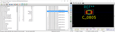
CvPCB, with another window open allowing you to view the footprints
It’s like the cloud, only not completely worthless
CvPCB is a new feature for KiCad 4.0. Instead of every other PCB design tool we’ve taken a look at so far, KiCad effectively stores all of the footprints in Github. In the Github repo for KiCad, you’ll find a bunch of files with a .pretty file name. These are the footprints for nearly every component you can imagine. If you’re running a fresh install of KiCad, everything shows up in CvPCB automagically – there’s nothing you need to worry about, and footprintsjust happen.
There’s a subtle brilliance about this implementation. It’slikethe cloud, only it’s completely verifiable, and if a part doesn’t work, you can fix it and submit a pull request. Already, this is phenomenally better than the Eagle paradigm, where millions of footprints are available in thousands of different libraries scattered around the Internet. If you’re reading through this series in order, take note: this ‘Github as the cloud’ will be a major point of comparison when we get to other cloud-based PCB design tools.

With that said, we need to associate footprints with the symbols on our schematic. To do that, go down the list in the center of the CvPCB window that contains a list of all the components in our schematic and associate a footprint with each part. Footprints are on the right, libraries (or categories) are on the left. To view the selected footprint in a new window, click the ‘view selected footprint’ button.
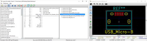
Selecting a footprint for the USB port
Getting Libraries In Order

The footprint editor window

The footprint editor, found in the launcher
This project is using (mostly) all through-hole parts, and as such, I could easily select a DIP8 footprint for the ATtiny85 and be done with the whole thing.This is a tutorial, though, and I need to demonstrate how to make a part – schematic and PCB view – from scratch.
To make a footprint, KiCad offers a Footprint Editor. This can be accessed from either PCBnew or the launcher. Click on that, select File -> New Footprint, enter a name for this footprint (‘ATtiny85’ will do), the name of the footprint and a reference designator is placed onto the footprint editing window.

Libraries are important, and since KiCad is now running on ‘not-worthless cloud technology’, we have to create a library for this project that won’t be saved along with our copies of the standard Github libraries. Select File -> Save Footprint In New Library,savethis library wherever the rest of the files are for this project, and give the library a name.
We have just created a new library, but that doesn’t mean KiCad knows what library we’re working with. In the Footprint Editor, select Preferences -> Footprint Libraries Manager, and click on the ‘Project Specific Libraries’ tab. Hit the ‘Append Library’ button, and drop the path to the library we just created in the ‘Library Path’ field. That’s more KiCad weirdness, but once we’re done we can finally create a footprint.

Making The Footprint
Now that we have the Footprint Editor open, a part name and a reference for the footprint, and the library all set up, it’s time to actually put some pads down. There are a few relevant buttons on the screen:

Add a pad

Add a line

Add an arc

Add a circle
The most important, obviously, is the ‘Add a pad’ button. Click that and drop some pads down where they should be. This is a standard DIP8, or two rows of four pins 0.3″ apart. The default grid, as you may have noticed, is 50mils.


After placing the pads, use the hotkey ‘E’ to edit the properties of each pad. Here, you can change a through-hole part to an SMD, change the dimensions of the pad, hole, and shape of everything. Importantly, the Pad Properties window allows you to change thenumberof the pad. The number of the pad is how KiCad connects the schematic representation of a part with the footprint. Get this right, or else nothing will work.
Add a few lines to the footprint, save your work in the project library, and go back to the schematic. You’re done. That’s how you make a footprint.
From Schematic To Board
Now that the schematic has footprints associated to everything, it’s time to open up PCBnew, move parts around, and put some traces between parts. Do that. Oh, nothing shows up. Why is that?You need to generate a netlist in the schematic view, and import it in PCBnew. There’s a button with ‘NET’ written on it in both programs. Click those. Now, what do we get when the netlist is successfully imported into PCBnew? The worst mess you’ve ever seen in any sort of design program:

I desperately want to see someone import a netlist for a large project in KiCad.

We end up with a gigantic mess on our hands. No worries, ‘M’ is the hotkey to move the parts around. You can also use the ‘Move Footprint’ mode to automagically place these parts. Reference the PCB we designed for the introduction to this series and move some parts around until we get something resembling the board below. The relevant hokeys are ‘M’ for move and ‘R’ for rotate. As always, there’s the ‘?’ hotkey that tells you everything you need to know.

That’s close, but it looks horrible. Deselect Footprint mode, use your cursor, and move all those labels and references around. We don’t need “CONN-01×04” on the board, and it’s really helpful to have the values of resistors inside their own footprint. With a little bit of work and deleting those labels, you’ll have something that looks like this:

Holy crap, that actually looks like something. All the resistors and diodes are labeled with their value, all the superfluous references are gone, and thisactually looks good.You can’t do this in Eagle easily.

With the layoutpretty muchfigured out, it’s time to finally draw some traces. This requires a description of the layers.
F.Cu and B.Cu are the top and bottom copper layers. The hotkeys for these layers are PgUp and PgDn
Edge.Cuts is the equivalent of the ‘Milling’ layer in Eagle. This is the outline of your board.
F.SilkS and B.SilkS is the silkscreen – the text and outlines of your components.
F.Mask and B.Mask is the soldermask. It’s usually green, or purple from OSHPark.
F.Adhes and B.Adhes is glue applied to SMD components.
F.Paste and B.Pasteis where solder paste will be applied.
For a simple board that won’t be sent off to an assembly house, the only layers you need to worry about are the copper layers, the Edge.Cuts, and the silkscreen.
The first thing to do to complete the board is to draw the ‘edge’ or milling layer. Select the ‘Add a graphic line’ button on the right hand toolbar, and draw a rectangle around all our parts. That’s simple enough.
Now it’s time to actually put some traces down. You can select which copper layer to use in the top toolbar, and the relevant hotkey is ‘X’. Hit ‘X’, click on a few airwires, and route them just like the reference PCB. Don’t worry about power or ground traces – we’re going to do those with copper fills. When you’re done, you should have something like this:


That’s pretty much all there is to it, save for the copper fills. To do that, we need to add a ‘filled zone’ or ‘copper pour’ or a ‘polygon’. By any other name, it’s just a big area of copper that is connected to a single net in the schematic.
Click on the ‘Add filled zones’ button, and a ‘Copper Zone Properties’ window will show up. Here, you can assign a layer of copper to a specific signal. Our board puts +5V on the back copper, and GND on the front copper. In the Copper Zone Properties, select the B.Cu layer, the +5V net, hit Ok, and trace around the edge of the board. Do the same with the F.Cu layer and the GND net. When those fills become hatches around the edges of the board, hit the ‘B’ hotkey to render the copper fills.


That’s it. We aretechnicallydone. If you save and drag the.kicad_pcbfile onto the OSHPark web page you’ll get a pretty purple PCB in a week or two. That’s not to say this PCB actually works – I screwed up the USB signals in the schematic, and that propagated over to the PCB. No matter, because no one is actually going to build one of these boards.
This just about concludes the ‘Creating A PCB in Everything’ tutorial for KiCad. If you’ve been reading along for the last five thousand words, you have an excellent introduction to KiCad, and should at least be able to build a breakout board. This doesn’t mean I’m done with KiCad quite yet – there are a few more tricks to go over including DRC and ERC, a demo ofhow freakin’ awesomethe routing in KiCad is, and I need to put a keepout on the decoupling cap in on the board, anyway. Creating a PCB in Everything: KiCad Part 3 (the optional part) will be out sometime next week.
Thoughts on KiCad
This series of posts serves two purposes. First, it is a quick tutorial for various PCB design tools. After reading these posts, you should be able to guess your way through a PCB design tool and build a simple PCB. Second, each of these tutorials serves as a pseudo-review of each PCB design tool. Each of these posts serves to illuminate the quirks of a PCB design tool, and serves as a notice that I still have an unclaimed bounty for the first person to create a part for an ATtiny85from scratchin Fritzing. Don’t use Fritzing, it sucks.
Coming from Eagle, KiCad is downright weird. That’s not to say it’s difficult, though – it’s generally the same as any other PCB design tool. The interface, like nearly every Open Source project, is obtuse, and there are five non-obvious ways to complete any task. There is zero reason why parts imported from a netlist into a board are squished together. Custom libraries can and should be automatically imported. The KiCad community especially rancorous. The UI suffers from an intangible wrongness about it, although that seems to lessen after working with it for a few hours. In a sense, KiCad is exactly what you would expect from an Open Source project that is decades old, very mature, and has features packed to the gills: it’s very powerful, but not friendly to the beginner.
Although the KiCad beginner will struggle to wrap their heads around the interface, it will be one of the most powerful PCB design tools I’ll use in this series of posts. No other free (beer) program will give you 32 copper layers and unlimited routing space. Nothing else uses the cloud/GitHub like KiCad. It’s brilliant.
A few months ago, if someone asked me to suggest a PCB design tool, I’d give Eagle or KiCad as suggestions. Eagle is easy enough to learn, and will be getting better since the Autodesk acquisition. KiCad is robust, and even in the best case of Eagle development, Autodesk may only ever reach parity with what KiCad can do.
Now, KiCad is growing on me. I have a secret project where I need to build and manufacture a thousand relatively complex boards. My previous go-to was Eagle, but I think I’m going to do this board in KiCad.


potluck9
2/11/2017 10:06:30 AM
Remarkable.It help me a lot. Thank you.