 My Message
 Suggestions


Considerable signal reflection and falsification will occur, thus resulting in design failures if there is no impedance control in the PCB. Normal signals, such as PCI bus, pci-e bus, USB, Ethernet, DDR memory, LVDS signal, etc. also require impedance control. Finally, PCB design will be achieved by impedance control and it can put forward for PCB technology. After talking with PCB manufacturers and combining with the use of EDA software, the trace with impedance control can be made according to the integrity of signal.
Different routing methods can be calculated to obtain the corresponding impedance.

Microstrip line
It is composed of a ribbon conductor and ground plane, with dielectric in the middle. If the dielectric constant of the dielectric, the width of the line, and the distance to the ground plane are controllable, the characteristic impedance of the dielectric is also controllable, and the accuracy is less than + / -5%.
Stripline
A strip is a strip of copper between two conductive surfaces. If the thickness and width of the line, the dielectric constant of the medium, and the distance of the ground plane of the two layers are all controllable, then the characteristic impedance of the line is also controllable, and the precision is within 10%.
Multi-layer structure
In order to control the impedance of PCB well, the structure of PCB should be understood first.
Generally, the multi-layer board is formed by lamination and lamination of the core board and semi-solidified sheet. The core board is a kind of rigid, specific thickness and copper plate, which is the basic material of the printed board. The semi-solidified sheet constitutes the so-called infiltration layer, which ACTS as a bonding core plate. Although there is a certain initial thickness, the thickness will change during the pressing process.
The outermost layer of the multilayer board is the soldering layer, which is often called "green oil". Of course, it can also be yellow or other colors. The thickness of the solder barrier is generally difficult to determine accurately. The area without copper foil on the surface is slightly thicker than the area with copper foil.
When making a printing plate of a certain thickness, on the one hand, it is required to select the parameters of various materials reasonably; on the other hand, the final forming thickness of the semi-cured sheet is smaller than the initial thickness. Here is a typical six-layer laminated structure:
PCB parameters
In different PCB plants, there will be slight differences in PCB parameters. Through communication with technical support of PCB plants, some parameters data of PCB factories can be obtained.
Copper foil: there are three types of copper foil that can is commonly used: 12um, 18um and 35um. The final thickness is about 44um, 50um and 67um after finished products are made.
Core plate: the common material are S1141A, the standard FR-4, and two bread copper. The specification can be chosen and confirmed with the PCB manufacturer.
Semi-curing tablet
The specification (original thickness) is 7628 (0.185mm), 2116 (0.105mm), 1080 (0.075mm) and 3313 (0.095mm). The thickness after actual pressing is usually about 10-15um smaller than the original value. The same infiltration layer can use up to three semi-cured tablets, and the thickness of three semi-cured tablets can not be the same, at least one semi-cured tablets, but some manufacturers require at least two.
If the thickness of the semi-cured sheet is insufficient, the copper foil on both sides of the core plate can be etched off, and then the semi-cured sheet can be used to adhere on both sides, so that a thicker infiltration layer can be achieved.
Resistance welding layer: the thickness of the resistance welding layer on the copper foil is C2 (38-10um), while the thickness of the resistance welding layer on the surface of no copper foil area is C1 (413-15um) according to the thickness of the surface copper. When the thickness of the surface copper is 45um, C1 (17-18um) is when the thickness of the surface copper is 70um.
Cross section of a wire: we think of the cross section of a wire as a rectangle, but it's actually a trapezoid. Taking the TOP layer as an example, when the thickness of copper foil is 1OZ, the upper base of the trapezoid is 1MIL shorter than the lower base. For example, if the line width is 5MIL, the upper base is about 4MIL and the lower base is about 5MIL. The difference between the upper and lower base sides is related to the thickness of copper.
Dielectric constant: the dielectric constant of semi-solidified sheet is related to thickness.
The dielectric constant of the plate is related to the resin material used, the dielectric constant of FR4 plate is 4.2-4.7, and will decrease with the increase of frequency.
Dielectric loss factor: the energy consumed by a dielectric material under an alternating electric field is called dielectric loss. The typical value of S1141A is 0.015.
Minimum wire width and spacing to ensure processing: 4mil/4mil.
Introduction to impedance computing tools
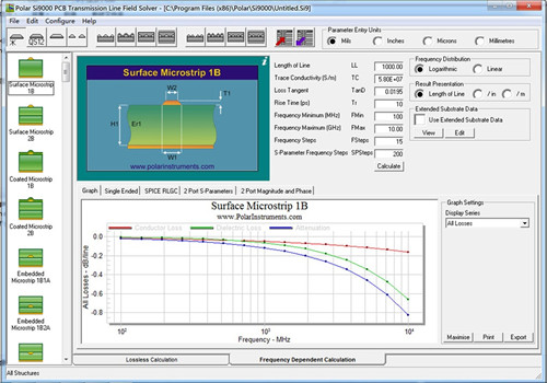
When we understand the structure of the multi-layer board and master the required parameters, we can use EDA software to calculate the impedance. Allegro can be used for calculations, but another tool is recommended here, Polar SI9000, which is a good tool for calculating characteristic impedance.
Whether it is a difference line or a single terminal line, when calculating the characteristic impedance of the inner layer signal, you will find that there is only a small gap between the results of Polar SI9000 and Allegro, which is related to some details, such as the shape of the cross section of the wire.
But if the characteristic impedance of Surface signal is calculated, I suggest you choose Coated model instead of Surface model, because this model considers the existence of resistance welding layer, so the result will be more accurate. The following figure is a screenshot of the surface differential line impedance using Polar SI9000 in consideration of the solder barrier.
Since the thickness of the resistance welding layer is not easy to control, an approximate approach can also be used according to the recommendations of the plate factory: subtract a specific value from the result of the Surface model calculation, and recommend the difference impedance minus 8 ohms, and the single-end impedance minus 2 ohms.
Differential PCB requirements for routing
1. determine routing mode, parameters and impedance calculation. The difference method can be used to calculate the impedance using the correlation impedance calculation software (such as POLAR-SI9000) or the impedance calculation formula.
2. parallel isometric lines. Determine the line width and spacing, and strictly follow the calculated line width and spacing when walking the line. There are two ways of parallelism: one is for two lines to go on the side-by-side, and the other is for two lines to go on the over-under.
Generally try to avoid using the difference signal between the layers, namely because in the actual processing of PCB in the process, due to the cascading laminated alignment accuracy is much lower than provided between the etching precision, and in the process of laminated dielectric loss, cannot guarantee difference line spacing is equal to the thickness of the interlayer dielectric, will cause the difference between the layers of the difference of impedance change. Therefore, it is recommended to use differences within the same layer as far as possible.


