 My Message
 Suggestions


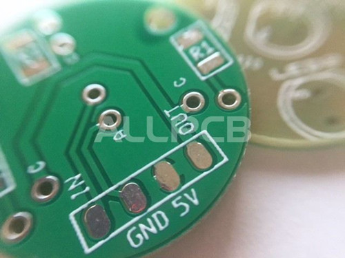
PCB substrates are generally classified by the insulating part of the substrate. Common raw materials are electric wood boards, fiberglass boards, and various types of plastic boards. Manufacturers of PCBs generally use an insulating part composed of glass fiber, non-woven material, and resin, and then press it into a "prepreg" with epoxy resin and copper foil.
The following problems may occur in the substrate during the PCB design process.
Symptoms of various soldering problems: There are blast holes in cold solder joints or solder joints.
Inspection method: The hole is often analyzed before and after dip soldering to find out where the copper is stressed. In addition, the raw material is subjected to the feed inspection.
The copper-clad board must be inspected before the warehouse is inspected. Check whether the board surface has scratched or exposed substrate. If it is necessary, contact the supplier in time and make appropriate treatment according to the actual situation.
The copper clad plate is scratched during the cutting process. The main reason is that there is a hard object in the machine surface. When the copper plate and the sharp object are rubbed during the material opening, the copper foil is scratched to form the exposed substrate. The countertop must be carefully cleaned before the material to ensure that the countertop is smooth and free of hard objects. When the machine operate, formed by the following tips of the drill bit .
a. The clip can be replaced by the number of times the knife is recorded or according to the degree of wear of the clip;
b. Clean the clamps regularly according to the operating procedures to ensure that there are no debris in the clamps.
The board is scratched during the transfer process:
When the board is lowered, it is not properly placed. In order to reorganize it, the board is pushed hard, causing friction between the board and the board to scratch the board surface.
After sinking copper, the whole board is plated after plating, due to improper operation is scratched:
After the copper is deposited and the plate is plated after plating, since the plates are stacked together, when there is a certain amount, the weight is not small. When the plate is lowered, the plate angle is downward and a gravity acceleration is added to form a strong impact force. Impact on the surface of the board, causing the surface of the board to scratch the exposed substrate.
The production board is scratched when it passes the horizontal machine:
a. the baffle of the grinding machine sometimes touches the surface of the plate, the edge of the baffle is generally not flat and the object is convex, and the surface of the baffle is scratched when passing the plate;
b. The stainless steel drive shaft is made into a pointed object due to damage. When the plate is passed, the copper surface is scratched to expose the substrate.
Possible reason:
Blast holes or cold solder joints are seen after the soldering operation. In many cases, the copper plating is poor, and then expansion occurs during the soldering operation, causing holes or blast holes in the metallized hole walls. If this is produced during the wet processing process, the absorbed volatiles are masked by the coating and then driven out under the heat of the dip soldering, which creates a spout or blasthole.
Solution:
Try to eliminate copper stress. The expansion of the laminate in the z-axis or thickness direction is generally related to the material. It can cause the metallized holes to break. Advice with laminate manufacturers to obtain materials with less z-axis expansion.
The bond strength problem phenomenon: In the dip soldering process, the pad and wire are detached.
Inspection method: During the inspection of the feed, fully test and carefully control all wet processing processes.
Possible reason:
1. The delamination of the pad or wire during processing may be due to plating solution, solvent etch or copper stress during the plating operation.
2. Punching, drilling or perforating will cause the pad portions to detach, which will become apparent during the hole metallization operation.
3. During wave soldering or manual soldering operations, pad or wire detachment is usually caused by improper soldering techniques or excessive temperature. Sometimes the laminate or wire is detached because the laminate is not properly bonded or the thermal peel strength is not high.
4. Sometimes the design wiring of the printed board causes the pads or wires to detach in the same place.
5. During the soldering operation, the retained heat of absorption of the component causes the pad to detach.
Solution:
1. Give the laminate manufacturer a complete list of solvents and solutions, including the processing time and temperature for each step. Analyze whether the plating process has copper stress and excessive thermal shock.
2. Obey the mechanical processing methods of pushing and depositing. The metallized holes are often analyzed to control this problem.
3. Most of the pads or wires are disconnected due to the lack of strict requirements for all operators. Failure of the solder bath temperature test or extension of the residence time in the solder bath can also occur. In the manual soldering trimming operation, the pad detachment was probably due to the use of improper wattage of electric ferrochrome and the failure to perform professional process training. Some laminate manufacturers now manufacture laminates with high levels of peel strength at elevated temperatures for use in stringent soldering.
4. If the detachment caused by the design and wiring of the printed board occurs in the same place on each board; then the printed board must be redesigned. Usually, this does happen in thick copper foil or wire corners. Sometimes, such a phenomenon occurs with long wires; this is because of the difference in thermal expansion coefficient.
5. PCB design time. Remove the heavy components from the entire printed board, if possible, or after the dip soldering operation. The soldering iron is usually carefully soldered with a low wattage soldering iron, which is shorter than the component dip soldering.
The size of the excessive change problem phenomenon: the size of the substrate after machining or soldering is out of tolerance or can not be aligned.
Inspection method: Full quality control during processing.
Possible reason:
1. The direction of the texture of the paper-based material is not noticed, and the forward expansion is about half of the transverse direction. Moreover, the substrate cannot be restored to its original size after cooling.
2. If the local stress in the laminate is not released, it sometimes causes irregular dimensional changes during processing.
Solution:
1. The entire production staff often cuts the sheet in the same structural texture direction. If the dimensional change is outside the allowable range, consider using a substrate instead.
2. Contact the laminate manufacturer for advice on how to release material stress prior to processing.


