 My Message
 Suggestions


Let's face it. We all make mistakes, and PCB designers are no exception. And contrary to popular belief, making mistakes is ok, as long as we learn from them. Here is a quick summary of some common PCB mistakes.

1. Choose the wrong PCB design software
Confucius said, “A man who does not plan long ahead will find trouble at his door.” This applies to PCB design too. One of the first steps to successful PCB design is to choose the right tools. There are many powerful and easy-to-use electronic design automation (EDA) software packages available for PCB designers today. Each one has its own unique capabilities, advantages and limitations. You should also be mindful that no software is infallible, so issues such as component footprint mismatch can and do occur. Although there may not be a single tool that meets all of your needs, you should do your homework to find the best fit for your requirements.
2. Poor communication with designer and/or manufacturer
Even though out-sourcing of PCB design is becoming more common, and is often more cost-effective, it might not be the ideal solution for highly complex PCB designs where performance and reliability are key. As the complexity of designs increase, the face-to-face time between the engineer and PCB designer to ensure precise component placement and routing in real-time becomes very important and can help to eliminate costly rework later.
It is equally important to engage the PCB board manufacturer early on in the design process. They can provide initial feedback on your design to maximize efficiencies based upon their processes and procedures that will save you time and money in the long run. By making them aware of your design objectives and involving them in the early stages of PCB layout, you can avoid any potential problems long before going into production and shorten time-to-market.

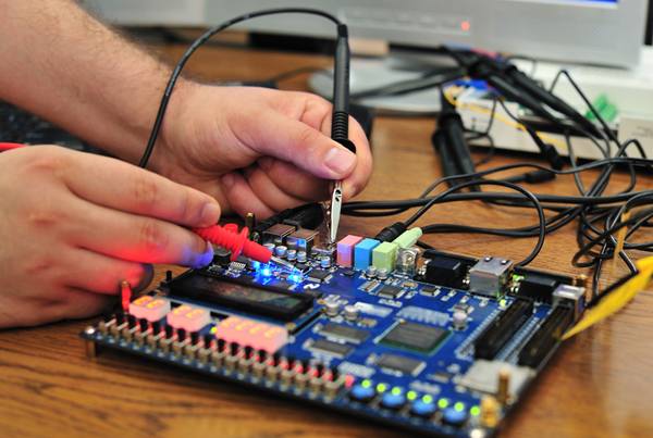
3. Failure to test early prototypes
Prototype boards allow you to prove that your design works according to your original specifications. Prototype testing allows you to validate the functionality and quality of the PCB and its performance before it is mass-produced. Successful prototype testing requires a good deal of time and experience, but by starting with a robust test plan and a clear set of objectives evaluation time can be decreased, and the likelihood of production-related mistakes reduced. If any issues are found during prototype testing, a second iteration of tests on a reconfigured board will need to be performed. By including high-risk elements early in the design process, you will be able to benefit from multiple iterations of testing and identify any potential issues early on, reducing risks and ensuring project deadlines are met.
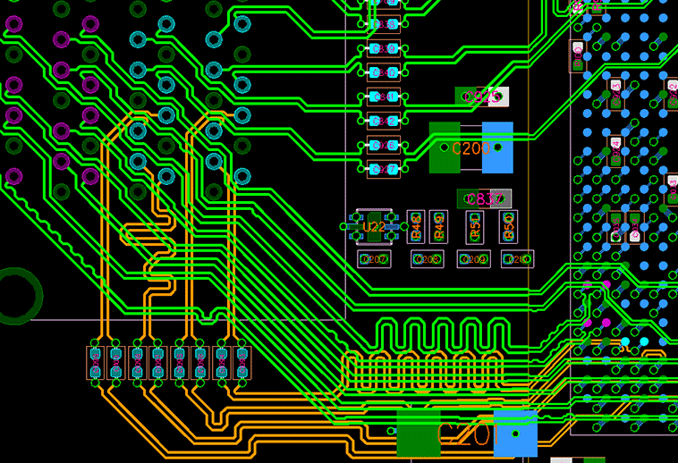
4. Using inefficient layout techniques or incorrect components
The demand for smaller and faster devices requires PCB designers to layout complex designs in significantly reduced footprints using smaller components that must be placed closer together. Making use of technologies such as embedded discrete devices on inner PCB layers or smaller pin pitch ball grid array (BGA) packages will help to reduce the board size, improve performance and leave room for rework when issues are encountered. When working with components that have higher pin count and smaller pitch, it is important to select the right board layout technique in the design stage to avoid problems later on and minimize fabrication costs.
Also be sure to carefully study the range value and performance characteristics of any substitute components that you plan to use, even those that are labeled as drop-in replacements. A slight variation in the characteristics of the substitute component may be enough to throw off the performance of your entire design.
How about you? Have you made some PCB design mistakes in the past that have made you a better designer today? Feel free to comment and provide a few more mistakes of your own so that others can learn from them too.


Alex Alfonso
1/23/2017 6:20:55 AM
Glad to read such a marvelous article here. You are a genius.