 My Message
 Suggestions


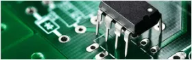
[Erich Styger] was bit by a nasty gotcha when soldering a QFN surface mount chip. The problem rears its ugly head when combining a chip possessing a padless conductor and a PCB without a solder mask. As you can see in the image above, there is a conductor exiting the side of the plastic QFN, but there is no pad associated with it. For this reason, you won’t see the conductor documented in the datasheet as a pin. It is documented in the mechanical drawing of the package, without any explicit reference to its existence. This is the Jason Bourne of package quirks.

The PCB layout just happens to have a trace exiting right under this conductor. The two aren’t touching, but without solder mask, a bit of melted metal was able to mind the gap and connect the two conductors. [Eric] notes that although the non-pad isn’t documented, it’s easy to prove that it is connected to ground and was effectively pulling down the signal on that trace.
In a recent article on Hackaday I talked about “dangling pointers” and the challenge when interrupts expose the bug. [Erich’s] covered a ton of posts about embedded software. I was doing some poking around and was delighted to find that he covered the same concept and a solution for it using a program calledcppcheck.


Gabe
2/17/2017 4:58:38 AM
Please keep doing your great job.
Bernie
2/17/2017 4:58:38 AM
I must say you have very interesting posts here.