My Message
 Suggestions


What is a via?
Via is one of the important components of a multi-layer PCB. The cost of drilling is usually 30% to 40% of the cost of PCB board. Simply put, every hole in the PCB can be called a via.
In terms of function, the vias can be divided into two types: one is used as an electrical connection between the layers; the other is used for fixing or positioning the device. If the process is in the process, the vias are generally divided into three types, namely, blind vias, buried vias, and vias.
The blind holes are laid out on both sides of the PCB and with a deepness for the joint of the trace. Buried holes points to a joint hole placed in the inner layer of the PCB. The above 2 kinds of holes are placed in the inner layer of the PCB.
The third type is called a through hole, and the hole passes through the entire circuit board and can be used to implement internal interconnection or as a mounting hole for the component.
Since the via is easier to implement in the process and lower in cost, it is used in most printed circuit boards without the need for two other vias. The via holes described below are considered as through holes unless otherwise specified.
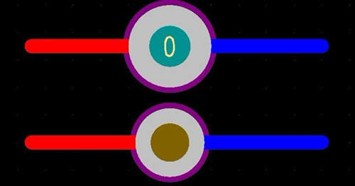
Via composition
From a design point of view, a via is mainly composed of two parts, one is the middle hole, and the other is the pad area around the hole. The size of these two parts determines the size of the vias. Visibly, in complex board layout, the smaller holes are better, so that more wiring space can be left on the board. In addition, the smaller the via, its own parasitic capacitance. The smaller, the more suitable for high speed circuits.
However, the reduction in the size of the hole also brings about an increase in cost, and the size of the via hole cannot be reduced indefinitely. It is limited by the process technology such as drilling and plating: the smaller the hole, the more time it takes to drill the hole.
The longer it is, the easier it is to deviate from the center position; and when the depth of the hole exceeds 6 times the diameter of the hole, there is no guarantee that the hole wall can be uniformly plated with copper. For example, the thickness of a normal 6-layer PCB (through-hole depth) is about 50Mil, so PCB manufacturers can provide a minimum diameter of 8 Mil.
Parasitic characteristics of vias
1. Parasitic capacitance
The via hole itself has a parasitic capacitance to the ground. If the via hole diameter of the via hole on the ground layer is known to be D2, the diameter of the via pad is D1, the thickness of the PCB board is T, and the dielectric constant of the board substrate is ε, the parasitic capacitance of the via is similar to:
C=1.41εTD1/(D2-D1)
The main effect of the parasitic capacitance of the via on the circuit is to extend the rise time of the signal and reduce the speed of the circuit.
For example, for a PCB with a thickness of 50Mil, if a via with an inner diameter of 10Mil and a pad diameter of 20Mil is used, and the distance between the pad and the ground copper area is 32Mil, we can approximate the via hole by the above formula. The parasitic capacitance is roughly:
C=1.41x4.4x0.050x0.020/(0.032-0.020)
=0.517pF
The amount of rise time caused by this part of the capacitance is:
T10-90=2.2C(Z0/2)=2.2x0.517x(55/2)
=31.28ps

2. Parasitic inductance
Parasitic inductance exists in the via hole and there is parasitic inductance. In the design of high-speed digital circuits, the parasitic inductance of the via hole is often more harmful than the parasitic capacitance. Its parasitic series inductance weakens the contribution of the bypass capacitor and reduces the filtering effectiveness of the entire power system. We can simply calculate the parasitic inductance of a via approximation using the following formula:
L=5.08h[ln(4h/d)+1]
Where L is the inductance of the via, h is the length of the via, and d is the diameter of the center bore.
It can be seen from the equation that the diameter of the via has less influence on the inductance, and the greatest influence on the inductance is the length of the via. Still using the above example, the inductance of the via can be calculated as:
L=5.08x0.050[ln(4x0.050/0.010)+1]
=1.015nH
If the rise time of the signal is 1 ns, then the equivalent impedance is:
XL=πL/T10-90=3.19Ω
Such impedance can not be ignored in the presence of high-frequency current. It is important to note that the bypass capacitor needs to pass through two vias when connecting the power supply layer and the ground plane, so that the parasitic inductance of the via will be multiplied.
Tips for designing vias
Through-hole design in high-speed PCBs Through the above analysis of the parasitic characteristics of vias, we can see that in high-speed PCB design, seemingly simple vias often have a large negative effect on the design of the circuit. In order to reduce the adverse effects of parasitic effects of vias, we can try to do as much as possible in the design:
From the perspective of cost and signal quality, choose a reasonable size of the via size. For example, for 6-10 layer memory module PCB design, 10/20Mil (drill/pad) vias are better. For some high-density small-size boards, you can also try 8/18Mil. hole.
Under current technical conditions, it is difficult to use smaller size vias. For vias for power or ground, consider using larger sizes to reduce impedance.
The two equations discussed above can be concluded that using a thinner PCB board facilitates reducing the two parasitic parameters of the via.
The signal traces on the PCB should not be changed as much as possible, that is, try not to use unnecessary vias.
The power and ground pins should be punched in close proximity, and the shorter the leads between the vias and pins, the better, because they cause an increase in inductance. At the same time, the power and ground leads should be as thick as possible to reduce the impedance.
Especially in the case of very high via density, it may cause a broken channel in the copper layer to form a partition circuit. To solve such a problem, in addition to moving the position of the via, we can also consider the via in the copper layer. The pad size is reduced.