 My Message
 Suggestions


For the next post in the Creating A PCB series, we’re going to continue our explorations of Eagle. In Part 1, I went over how to create a part from scratch in Eagle. In Part 2, we used this part to create the small example board from the Introduction.
This time around I’ll be going over Design Rule Check (DRC) — or making sure your board house can actually fabricate what you’ve designed. I’ll also be covering the creation of Gerber files (so you can get the PCB fabbed anywhere you want), and putting real art into the silkscreen and soldermask layers of your boards.
The idea behind this series is to explore different EDA suites and PCB design tools by designing the same circuit in each. You can check out the rest of the posts in this series right here.
DRC – Design Rule Check
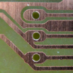
What happens when you don’t run a DRC. Image credit: Quinn Dunki
Board houses can’t produce PCBs with infinite resolution. There are limits to their process and when designing a PCB you can’t put traces too close together. The limits for each board house should be available somewhere on their web page, but generally you’re looking at a minimum trace width of 6 to 8 mil, a minimum trace separation of 6 to 8 mil, and a minimum drill size of 0.3 to 0.5 mm (about 12 to 20 mil). OSHPark is one of the better board houses with 5 mil width, 5 mil clearance, and 10 mil drills.
The Design Rule Check, or DRC, is how you find traces that are too small, too close together, or traces that simply overlap. This is how you check your board for errors before sending it off to a fab. That’s not to say the DRC in the current version of Eagle is good; KiCad has live DRC that is constantly checking your board. Eagle’s requires you to press a few buttons. This will change in the next few releases, though.
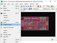
Get into the DRC by selecting ‘Tools’ -> ‘DRC in the board window. Something like this will pop up:

In the DRC window, you can set the minimum trace width for your project. The default is 8 mil, which is well within the capability of just about any board house. If you’re etching at home, you might want to bump this up a bit higher. For now, 8 mil separation is just fine, as are the rest of the default settings. Click through the tabs, and just see what options are available to you. There’s a ‘Check’ button at the bottom of this window. Click that, and you’re presented with all the errors you made.

When I ran the DRC on this project board, I had only one error relevant to this tutorial. The via I used to connect the VCC pin on the USB connector was too small. This drill was still well within the capabilities of OSHPark and Seeed, so I just clicked ‘Approve’. If your traces are too close together, or if they’re too close to a pad, the DRC will tell you.
It is imperative to run a DRC check before sending a board file off to a fab house. Not only will it help you stay within spec for the fab you are using, it will help catch silly errors that managed to get past you in the layout process.
Gerbers for Sending the PCB Off to Fab
If you’re only making two-layer boards and sending them off to OSHPark, Seeed, or DirtyPCBs, there is no need to do anything else to have your boards made. All of the usual online board houses accept Eagle .brd files. If you’re using any of these services, you can drag and drop your board file on the order page. It’s dead simple and almost foolproof.
But the Eagle .brd file is not the industry-standard way of having a board fabricated. If you ever need a thousand PCBs, are making 6 (or more) layer PCBs, or just have some strange requirement, you’ll want to consider Advanced Circuits, Gold Phoenix, and numerous other options for fabrication. That means you’ll have to turn your board into a Zip archive full of Gerber files.
‘Gerbers’ are a collection of files that define each layer of the board. The top layer of copper is its own file, the top silkscreen layer is its own file, the top soldermask is its own file, and if you’re extremely good, Gerber allows you to create a layer telling a robot where to apply solder paste.
Lucky for you — and because this guide is already too long — OSH Park has a wonderful guide along with the CAM files required to generate Gerber Files. I highly suggest using OSH Park’s CAM file for generating Gerbers. It will generate the following files:
Top Layer filename.GTL
Top Solder Mask filename.GTS
Top Silkscreen filename.GTO
Bottom Layer filename.GBL
Bottom Solder Mask filename.GBS
Bottom Silk Screen filename.GBO
Board Outline filename.GKO
Drills filename.TXT
Put all of these files into a folder and Zip it up. Inspect your Gerbers with one of a dozen different online Gerber viewers. That’s really all you need to know about generating Gerber files from your Eagle boards.
That’s Eagle.
In several thousand words and three posts, we’ve gone over how to create a new, custom part in Eagle, draw a schematic, place those parts onto a board, draw traces, and send that board off to a fab. This is the bare minimum of an introduction to Eagle CAD. Now we can knock Eagle off the list of How To Create A PCB In Everything.
For the next few posts in this series, we’ll be taking a look at Fritzing. If you’ve been reading along with this series, you already know the right way to make a PCB in Eagle. Fritzing will teach you the wrong way. As always, we’re looking for suggestions on what pieces of software we should cover next. If you have an idea, leave a note in the comments.


Livio
2/25/2017 8:35:40 PM
Great help to my new project.