 My Message
 Suggestions


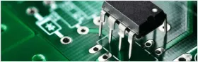
This is the continuation of a series of articles demonstrating how to Create A PCB In Everything. In this series, we take a standard reference circuit and PCB layout — a simple ATtiny85 board — and build it with different PCB design tools. Already, we’ve taken a look at the pre-history of PCB design with Protel Autotrax, we learned Fritzing is a joke for PCB design, and we’ve done a deep dive into Eagle. Each of these tutorials serves two purposes. First, it is a very quick introduction to each PCB design tool. Second, this series provides an overall comparison between different PCB design tools.
Now, finally, and after many complaints, it’s time for the tutorial everyone has been waiting for. It’s time for KiCad.
No, like the head of the Bajoran clergy
Although KiCad (pronounced ‘Kai-Cad’ like the head of the Bajoran clergy, not ‘Key-Cad’ like the thing that goes in a lock) is the new hotness when it comes to PCB design. The amazing growth of KiCad installations over the past few years is a long time coming. In development since 1992, KiCad has cemented itself as the premier Open Source PCB design suite, and since 2013 CERN has been making contributions to the project. More recently, the KiCad project has been showing off some amazing new features. These include 3D rendering of boards, interactive routing, push-and-shove, simulation, and dozens of other features that put it on a path to being on par with the top of the line EDA suites. Add in some great community contributions, and you have something really, really amazing. All of this is wrapped up in an Open Source license, free as in speech and beer. If you’re looking for the future of PCB design, Eagle is going to get very good but KiCad is almost there now while being Open Source.
The KiCad Overview
As I said in the introduction to this series of posts, this tutorial will be broken down into three main parts. The first will be how to create a part — specifically a DIP8 ATtiny85 — as a schematic symbol and how to create the schematic we need. The second part of this KiCad tutorial will assign footprints to our symbols and turn the schematic into a board you can send off to a fab house. Finally, we’ll take a look at the cool features of KiCad, such as push and shove routing and 3D rendering.
For this part of the KiCad tutorial, we will only concern ourselves with making a part for a DIP8 ATtiny85. Download KiCad and let’s get started.

Your first view of KiCad
Just like Eagle – and every other PCB design tool, for that matter – there are several different editors in KiCad. They are:
Eeschema – the schematic editor
The Schematic library editor – used for editing part libraries
Pcbnew – the ‘board’ editor
The PCB footprint editor – used for editing footprints (the physical package) of parts
An introduction to the terminology of PCB design might be in order. A schematic is the abstract design file, showing the electrical connections between all the components in your circuit. The schematic is not sent to the fab house.
A PCB or board describes the layout of the components, holes, pads, traces, connections, mechanical design, and silkscreen. Designing a board is the end game of all PCB design work, and it is this file that gets sent off to a fab house for manufacturing.

The schematic for our project

The board we will eventually build in KiCad. This board was made in Eagle.
Before we put together a schematic and design a board, we must learn how to build our own parts. To start, install KiCad, select File -> New Project, and name it ‘Nanite’, or ‘Some Trash I’ll Never Do’
Making A Part
All of these tutorials demand making a part from scratch. Right now, that means making a part and footprint for a DIP8 ATtiny85. From the main KiCad window, open up the Part Library Editor, and you have a window that looks like this:

When you first open the Part Library Editor, no libraries are loaded. You would think it would be possible to simplycreate a new library, and design some parts, but KiCad is weird. To make your own library in KiCad, you must first select an existing library and save it as your own. Yes, it’s a bit weird and one of the many oddities of the KiCad UX,but at least it’s better than Fritzing.

Click the ‘Create a new component’ opamp icon, and you’re presented with a window asking you to name your part. For small, simple, jellybean components, you won’t have to bother with anything except for the name. Name your part ATtiny85 and click okay. The name and designator of the part will be dropped into the window. Now we’re ready to add pins to our part.

Oh God Everything Is Backwards And My Mouse Doesn’t Do Anything

There’s a reason for this: KiCad, like almost every other PCB design tool, is based on hotkeys. This is the reason KiCad gets the reputation for not being user-friendly, but there’s a solution: just type a question mark. The list of hotkeys will pop up, and now you’ll always know what keys you need to hit to do what you want to do. To move the ‘ATtiny85’ and ‘U?’ label off to the side, hit ‘M’ while hovering the mouse over each label.

Now it’s time to add pins. Click the ‘Add pins to Component’ button on the right side of the window. Next, click anywhere on the Part Library Editor window.

The Pin Properties window is where you assign a name, number, and graphical style to all of the pins in the schematic representation of your part. We’re doing a very simple part with power and ground on one side, and all the IO on the other side. As long as the pin names are correct, and all the pins correspond to the correct numbers on the footprint, you shouldn’t have much trouble. The only thing that might trip you up is the orientation of the pins; here, the circle at the end of each pin designates where the pin connects to a net on the schematic.
Drop eight pins down and make your part look something like what we made in the Eagle tutorial. You’ll end up with something like this:

With the pins dropped into the window and correctly labeled, all we need to do to finish the part is to draw a rectangle. Click on the ‘draw a rectangle’ icon, click once in the corner, drag, and click again to finish the rectangle. Hit File -> Save Current Library, and we’re done making the schematic symbol for this part.
From Symbol To Schematic
Now that we have a symbol for the ATtiny85 we’re going to use in this board, it’s time to make a schematic. From the main KiCad window, open up the Electronic Schematic Editor, and you’ll be presented with the following window:

Again, the hotkeys are going to kill you. To add a component, press ‘A’. You might also want to hit ‘?’ and bring up the list of hotkeys.
At this stage, we’re not concerned with footprints, or the physical dimensions of the components we’re eventually going to place on the board. All we want aresymbols. There are hundreds of different varieties of USB connectors, but right now we don’t care. All we need to do is drop a few resistors, diodes, connectors, and other parts onto the schematic. To do that, press ‘A’, and the window below will pop up.

Since we’re directly copying the reference schematic from the introduction to this series, we need the following components:
- Two 1×4 connectors
- Two Zener diodes
- Four resistors
- One LED
- One USB port (OTG)
- One unpolarized cap
- One ATtiny85
- A smattering of +5V and GND symbols
For each of those components, press ‘A’ to add a part, search for the part, and drop it onto the schematic. If you’re really good, you can use the ‘P’ hotkey to add power and ground parts. When you’re done, you should have something that looks like this:

That looks about right
The important hotkeys to know are ‘A’ to add a part, ‘M’ to move a part, and now ‘W’ to add a wire between parts. Again, pressing ‘?’ displays a list of hotkeys. Of special interest is the ‘K’ hotkey to stop drawing a wire.

To label these wires and turn them into nets, use the ‘L’ hotkey, and select a name for each of your nets. Drop this label over the open connection on each wire to turn them into nets. When you’re done, you’ll have something that looks like this:


The Annotate Schematic tool automatically assigns a letter (D for diodes, L for inductors, R for resistors, Q for transistors…) to each part, along with a number. There are options to set how these numbers are assigned, but this is a very simple circuit and simply pressing the ‘annotate’ will suffice.
With that, our schematic is done. We haven’t set any footprints up for each part, and we haven’t even started on the board yet. This post is already two thousand words long, though, andHackaday readers havethe entire Internet has no attention span.
In the next part of this KiCad tutorial, we’re going to take a look at assigning footprints (the physical representation of components) to the parts in our schematic. We’re going to make a board, after which we’ll take a look at DRC, and a few of the neat tricks in KiCad including 3D rendering, turning the board into a bunch of Gerbers, and send off to a fab house.


madeo
2/25/2017 8:34:09 PM
very useful informations.