 My Message
 Suggestions


In this essay, we will have brief introduction of the common PCB design steps.
Preliminary preparation
Clearly design the target, select the selected device type, confirm the overall plan, and come up with a written design plan.
Prepare the schematic package library and PCB package library of the device. There is specific package information for every component. If there is no such thing in the base library, it must be searched from the Internet. If it is still not available, it can only be drawn by itself. Some package generation software can be used to do this. It should be noted that the package must be placed in the specified directory;
PCB design
This part is the main part of the board design, but if there are problems in the previous scheme, it will bring a lot of obstacles to the back, so a good solution is half successful. The next step is to design step by step.
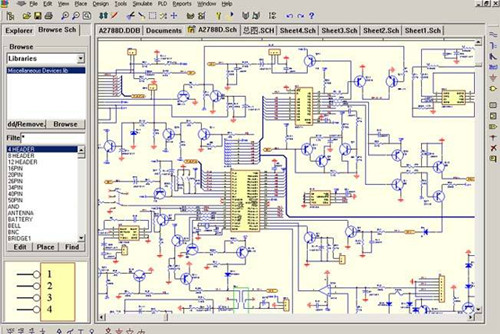
1. Schematic design
The workload of schematic design is not very large, but the importance is undoubtedly a correct schematic is the guarantee of the entire board function;
2. Create a schematic netlist
After the schematic is drawn, the netlist is generated and used for later import into the PCB drawing software. If cadence is used, the generated netlist file contains three files: pstxnet.dat/ pstxprt.dat/ pstchip.dat;
3. Create a mechanical design
Set related information such as PCB frame and height limit, and generate new mechanical drawing files and save them to the specified directory;
4. Read schematic net list
Read the schematic net list into PCB software such as Allegro;
5. Set basic information of the PCB board
Before starting layout and routing, you must first set the board layer, grid spacing, color and design constraints of the PCB board;

6. PCB layout
In addition to the very simple schematic, it is recommended to make a reasonable manual layout according to the functional distribution of the schematic. Manual wiring takes a long time, but it is more detailed and meets the actual requirements; automatic routing speed is fast but more over-control is used. It is generally recommended to manually route or combine the two methods;

7. Place test points
Place some voltage test points in the appropriate position to facilitate quick test confirmation after the board is fabricated;
8. Copper plating on the top and bottom
This step is not required, but almost all mature designs will be carried out. This not only strengthens the circuit board, prevents war page, but also enhances the shielding performance of the PCB board and improves the anti-interference ability of the PCB board;
9. Constraint rule checking
If some constraint rules are designed before the layout and routing, at this time, it is necessary to enter the constraint table for inspection, and whether all the routing designs are in compliance with the rules;
Post processing work
1. Adjust the board text
Add and adjust the silkscreen, and add some necessary information and company logo on the board;
2. Output illuminating files
Generate the correct illuminating file, you can use it to send the plate-making manufacturer for processing;
3. Document archiving
Commonly used reports are: component list, circuit board interface wiring table, printed circuit schematic and PCB board diagram.


