 My Message
 Suggestions


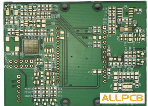
The so-called copper coating is to use the unused space on the PCB as the reference surface, and then fill it with solid copper, which is also called copper filling. The significance of copper coating is to reduce the ground line impedance, improve the anti-interference ability, reduce the voltage drop, improve the power supply efficiency, and connect with the ground wire to reduce the loop area.
There are some issues to be aware of when applying copper:
1. If the PCB has more ground, there are SGND, AGND, GND, etc., depending on the position of the PCB surface, the main "ground" is used as the reference to separate the copper, and the digital ground and the analog ground are separated. Copper is not enough to say, at the same time, before the copper coating, first increase the corresponding power connection: 5.0V, 3.3V, etc., thus forming a variety of different shapes of multi-deformation structure.
2. For a single point connection in different places, the method is to have a high resistivity and magnetic permeability through a 0 ohm resistor bead. It is equivalent to a series connection of a resistor and an inductor, but both the resistance value and the inductance are value vary with frequency.
It has better high-frequency filtering characteristics than ordinary inductors and resistive at high frequencies, so it can maintain high impedance over a wide frequency range, thus improving the frequency modulation filtering effect. As a power supply filter, an inductor can be used. The circuit symbol of the magnetic bead is the inductance.

However, it can be seen that the magnetic bead is used in the circuit function. The magnetic bead and the inductor are the same principle, but the frequency characteristics are different. The magnetic bead is composed of an oxygen magnet, and the inductance is composed of a magnetic core and a coil.
Composition, the magnetic beads convert the AC signal into heat energy, and the inductor stores the AC and slowly releases it. Magnetic beads have a great hindrance to high-frequency signals. The general specification is 100 ohms/100mMHZ, which is much smaller than the inductor at low frequencies.
3. Crystal oscillator: The crystal oscillator in the circuit is a high-frequency emission source. The method is to apply copper to the surrounding crystal oscillator, and then ground the crystal casing separately.
4. The problem of an isolated island (dead zone), if it feels great, it would not be a big deal to define a place to add it.
5. When starting the wiring, the ground line should be treated equally. When the line is routed, the ground line should be taken well. You cannot rely on the copper to remove the ground pin by adding a hole. This effect is very bad.
6. It is best not to have sharp corners on the board ("180 degrees"), because from the electromagnetic point of view, this constitutes a transmitting antenna! For other things that always have an effect, it's just big or small. I recommend using the edge of the arc.
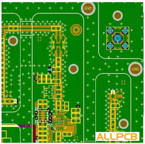
7. Do not apply copper to the wiring area of the middle layer of the multi-layer board. Because it is very difficult for you to make this copper "good grounding".
8. Metals inside the equipment, such as metal radiators, metal reinforcement strips, etc., must be “good grounded”.
9. The reflow area of the three-terminal regulator reduces the external electromagnetic interference of the signal.


