 My Message
 Suggestions


Tip 1: Focus on researching manufacturing methods and foundry chemical processing
In this era of fabless IC companies, it is not surprising that many engineers really don't know the steps and chemical processing involved in generating pcbs from their design files. This lack of practical knowledge often leads design novices to make more complex design choices that are not necessary.
For example, a common mistake that novices can make is to design a board layout with a particularly precise size, that is, using orthogonal wires associated with a tight grid. It turns out that not every board processing plant can produce it. A design that maintains sufficient reliability during the life of the field.
Factories with these capabilities may not be able to provide the most economical pcb price. Does design really need to be so complicated? Can board layouts be made on larger grids, reducing board cost and increasing reliability?
Other misunderstandings encountered by novice designers include too small via sizes and blind and buried vias. These advanced via structures are the product of powerful tools in the pcb designer toolbox, but their effectiveness is highly relevant to the specific situation. Just because they exist in the toolbox doesn't mean they should be used.
Tip 2: Believe in flying lines
Board schematic design takes a lot of time. Sometimes it takes a lot of time and it gives you the idea of skipping this process. However, in order to be able to design a complete circuit board in the future, you must have a patient learning schematic design.
First, a schematic is a visual description of a circuit that can exchange information at many levels. Subsections of the circuit can be drawn on several pages in detail, and components can be placed close to their function blocks regardless of their final physical layout.
Since each pin on each component is shown in the schematic symbol, it is easy to check for unwired pins. In other words, the schematic helps you quickly and visually determine this fact, regardless of whether the formal rules describing the circuit are followed.
In a discussion of the topic of stack overflow, a poster commented: "If a schematic might mislead people who look at it, then it must be a bad schematic, no matter what it ends up... in fact it is The correct schematic.
The problem is clear. The technically correct but confusing schematic is still a bad schematic." Although this view is easy to agree with, in the CAD program, an unreadable schematic can still be Expressing the connection information describing the circuit is still useful in layout design.
The conclusion is that when designing a pcb layout, having a schematic as a gold reference can make the job easier. Connect with symbols; you don't have to think about connections at the same time when dealing with routing challenges. Finally, I found that the wire connections you forgot to make in the first version of the design saved the number of redoes.
Tip 3: Use an autorouter, but don't rely solely on the autorouter
Most professional-grade pcb CAD tools have an autorouter. But unless you design the pcb to be professional, the autorouter will do the wiring at one time; for the pcb connection, the autorouter is not a one-click solution. You should still know how to do manual routing.
The autorouter is a highly configurable tool. In order to fully play their role, each task must be carefully and thoughtfully set for the router parameters, even for each module in a single pcb design must be set separately, there is no basic universal default settings for any occasion.
When you ask an experienced designer "what is the best autorouter", their usual answer is "the thing between your ears (eyes)", this is not a joke, they are serious. As a process, wiring is as artistic as an algorithm; wiring itself is heuristic, so it is very similar to traditional backtracking algorithms.
For constrained path selection applications (such as maze and jigsaw puzzles), backtracking algorithms are good for finding answers, but in open, unconstrained situations, such as pre-layout printed circuit boards of components, Backtracking algorithms are not good at finding the optimal solution.
Unless the autorouter constraints are highly detailed by the designer, the autorouter results still need to manually check for weaknesses in the backtracking algorithm results.
Wire size is another difficulty. The autorouter cannot reliably determine how much current will flow on a wire, so it can't help you determine how wide a wire to use. As a result, the wire width of most autorouters does not meet the requirements.
Many autorouters allow you to specify reference wire constraints. In a forum post on the stackexchange.com website, author Martin Thompson wrote, “I have used an autorouter for every board I am doing (sorry, a very high-end router...).
Your constraint is similar: only on this layer, the two signals form a differential pair. These networks must match the length, then you must tell these conditions to the autorouter.
" When you want to use the autorouter You have to ask yourself: "When I set the autorouter constraints for the board, maybe even set constraints on each wire in the schematic, how much manual wiring would this work be done?"
Experienced designers put a lot of effort into the original component layout, and almost half of the entire design time is used to optimize component placement:
1. Simplified wiring - minimize the intersection of flying lines, etc.;
2. Device proximity - shorter routing means better wiring;
3. Signal timing considerations.
In a user forum at Sunstone Circuits, a post wrote, "Pay attention to component layout. Component layout is easier to route. Component layout accounts for 70% of the total workload.
Before starting the first line Put all the components in place... Use flying leads (these lines indicate the connection that has not yet completed the wiring) as a rough guide to wiring complexity."
Older generations often use a hybrid approach to routing—hand-pick some important key lines and lock them when they are laid. The autorouter then handles non-critical conductors and helps manage the "escape state" in the routing algorithm. This approach is sometimes a good compromise between controlled manual routing and fast automated routing.
Tip 4: Board Geometry and Current
Most people who work in electronic design know that like a river going along a river, electrons may encounter throat points and bottlenecks. This has been directly applied in the design of automotive fuses. By controlling the thickness and shape of the wire (U-bend, V-bend, S-shape, etc.), the calibrated fuse will be blown at the throat when overloaded.
The problem is that pcb designers occasionally produce similar electrical throat points in their pcb design. For example: a 90 degree angle can be used where two fast 45s angles can be used; the curvature is greater than 90 degrees, forming a zigzag shape. In the best case, these wires reduce the speed at which the signal travels; in the worst case, they are like a car fuse and blow at the resistance point.
Tip 5: Oh, the pieces!
Fragmentation is a manufacturing issue that can be best managed with the right board design (Figure 1). In order to understand the fragmentation problem, we first need to review the chemical etching process.
The purpose of the chemical etching process is to dissolve out the unwanted copper. However, if there are particularly long, thin, strip-like pieces that need to be corroded, these pieces sometimes detach from the block before they are completely dissolved. This strip then floats in the chemical solution and may randomly land on another board.
The same risky situation is when the debris remains on the board. If the debris is narrow enough, the acid bath can corrode enough copper below to partially strip the debris. Now the debris is wandering around and attached to the board like a flag. Eventually it will fall on your own board, causing a short circuit to other wires.
So where do you go looking for potential debris and how to avoid them? When designing a PCB layout, it is best to avoid leaving a very narrow copper area (Figure 2). This area is usually caused by copper at the intersection of the wire and pad gap (Figure 3).
Set the minimum width of the copper to exceed the minimum allowed by the manufacturer, and your design should have no such problem. The standard minimum width for etching is 0.006 inches.
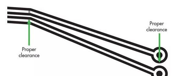
Figure 1: In this example, the narrow shield pattern between the wires appears to be very strong on the board substrate.
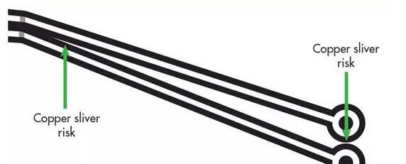
Figure 2: A very narrow sheet-like area, such as the one in the original design document, may be uncontrolled to peel off during manufacturing, creating short-circuit and yield problems.
Tip 6: Focus on DRC
Design Rule Check (DRC) is usually a perfect design by entering the manufacturer's production requirements. Although setting these requirements can be tedious, it is simple. Can help you better complete pcb development. Reduce the modification time.
It is precisely because of these specific rules that it is more conducive to the unity and convenience of internal procurement. This will greatly increase the efficiency of purchase and development.
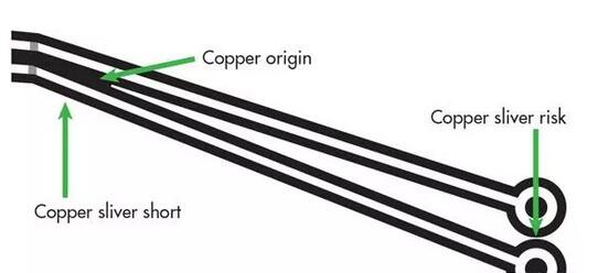
Figure 3: In this example, chemical etching changes the shape/size of the narrow strip fill. Unexpected scales and flaps can be produced when the fragments are peeled off.
To help solve all of these problems, many pcb design tools have built-in DRC checkers (some tools call them "constraints managers"), and the DRC checker interactively marks design rule violations when you are editing. Once you have set up the DRC rules for the chosen manufacturer, you should take the mistakes seriously.
DRC tools are generally conservative. They will intentionally report possible errors and let you make a decision. Screening hundreds of "possible" questions is tedious, but do it anyway.
The list of questions may have hidden reasons why the first production was doomed to fail. In addition, if your design generates a large number of possible errors, you should be aware that your routing may need to be improved.
Tip 7: Know the foundry you are using
After discussing DRC settings, this technique is almost – but not completely – superfluous. In addition to helping you properly establish DRC rules, knowing which OEMs your board will be sent to will also provide additional pre-manufacturing assistance.
A good foundry will provide some helpful help and advice before you place an order, including how to improve your design to reduce design iterations, reduce problems encountered during final commissioning on the test bench, and increase board yield.
Understanding the manufacturing process of printed circuit boards and understanding which processes and methods your manufacturers will use can help you make better design decisions.
Go visit your chosen supplier and see for yourself about the manufacturing process. Take advantage of the DFM (Manufacturability Design) tool before submitting your design to manufacturing.


