In the fast-paced world of electronics, ensuring the quality of printed circuit boards (PCBs) is critical. One of the most effective ways to reduce PCB manufacturing defects and maintain high standards is through In-Circuit Testing (ICT). But how exactly does ICT help in defect detection, and why is it a game-changer for minimizing issues like PCB assembly errors and poor solder joint inspection? In this blog, we’ll dive deep into the role of in-circuit testing applications and explain how they can elevate the reliability of your electronic products. Whether you’re an engineer or a manufacturer, understanding ICT is key to delivering flawless PCBs.
Let’s explore the ins and outs of ICT, from its fundamental principles to its practical benefits in catching defects early and ensuring top-notch quality.
What Is In-Circuit Testing (ICT) and Why Does It Matter?
In-Circuit Testing, commonly known as ICT, is a powerful method used to test individual components and connections on a PCB after assembly. Unlike other testing methods that focus on the overall functionality of a board, ICT zeroes in on specific elements like resistors, capacitors, and diodes to ensure they are correctly placed and functioning as expected. This makes it an essential tool for ICT for defect detection in modern PCB manufacturing.
The importance of ICT lies in its ability to catch PCB manufacturing defects early in the production process. By identifying issues such as open circuits, short circuits, or incorrect component values before the board moves to final assembly or shipping, ICT saves time, reduces costs, and prevents faulty products from reaching customers. For industries like automotive, medical, and aerospace, where reliability is non-negotiable, ICT is often a cornerstone of quality control.
Common PCB Manufacturing Defects and Their Impact
Before diving deeper into in-circuit testing applications, it’s important to understand the types of PCB manufacturing defects that can occur during production. These defects can lead to performance issues, product failures, or even safety hazards. Here are some of the most common problems:
- Short Circuits: These happen when unintended connections form between conductive paths, often due to excess solder or misaligned components. A short circuit can cause a board to overheat or fail entirely.
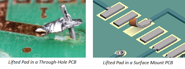
- Open Circuits: This defect occurs when there’s a break in the connection, preventing current from flowing through a circuit. It can result from broken traces or poor soldering.
- Component Misplacement: Incorrectly placed or oriented components can disrupt the functionality of the entire board.
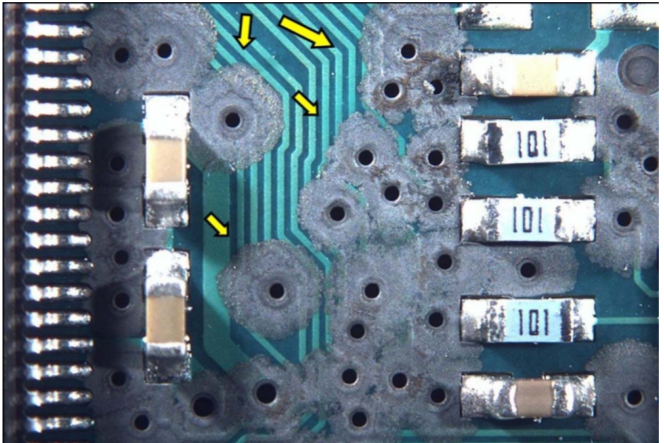
- Solder Joint Issues: Poor solder joint inspection can reveal defects like insufficient solder, cold joints, or cracks, which weaken connections and lead to intermittent failures.
- Incorrect Component Values: Using a resistor or capacitor with the wrong value can throw off the entire circuit’s performance, leading to unpredictable behavior.
The consequences of these PCB assembly errors can be severe, ranging from costly recalls to damaged brand reputation. This is where ICT steps in as a proactive solution to detect and address these issues before they escalate.
How In-Circuit Testing Works for Defect Detection
ICT operates by using a specialized test fixture equipped with probes that make contact with specific test points on the PCB. These probes measure electrical characteristics like resistance, capacitance, and voltage to verify that each component and connection meets the design specifications. Here’s a simplified breakdown of the ICT process:
- Test Fixture Setup: A custom fixture is designed for each PCB layout, with probes aligned to contact key test points on the board.
- Electrical Measurements: The ICT system applies small test signals (often in the range of 1-5 volts) to measure parameters like resistance (in ohms) or capacitance (in farads) at each point.
- Comparison to Standards: The measured values are compared against the expected values from the PCB design. Any deviation outside acceptable tolerances—such as a resistance reading of 10 ohms when 100 ohms is expected—flags a potential defect.
- Defect Reporting: The system generates a detailed report of any issues, pinpointing the exact location and nature of the defect for quick resolution.
By focusing on individual components and connections, ICT excels at detecting PCB assembly errors that might be missed by other methods like visual inspection or functional testing. For instance, it can identify a cold solder joint with a resistance reading higher than the typical 0.1-0.5 ohms, ensuring thorough solder joint inspection.
Key Benefits of ICT for Minimizing PCB Manufacturing Defects
Implementing ICT for defect detection offers several advantages that directly contribute to higher PCB quality and lower production costs. Let’s explore some of the standout benefits:
1. Early Detection of Defects
ICT catches issues at the assembly stage, long before the PCB is integrated into a final product. This early intervention prevents defective boards from progressing through production, saving significant rework costs. For example, fixing a short circuit during ICT might take minutes, while addressing it after final assembly could cost hours of labor and materials.
2. High Accuracy and Reliability
ICT systems are incredibly precise, often achieving fault coverage of over 90% for common defects like shorts and opens. By measuring exact electrical values—such as a capacitor’s rating within ±5% of the specified 10 microfarads—ICT ensures that even subtle issues are flagged before they cause problems.
3. Comprehensive Solder Joint Inspection
Poor soldering is a leading cause of PCB failures, but ICT excels in solder joint inspection. It can detect high-resistance joints or incomplete connections by analyzing impedance values, often identifying issues that visual inspections might miss. This ensures robust connections that withstand thermal and mechanical stress.
4. Reduced Testing Time for High Volumes
While setting up an ICT fixture can be time-intensive, the actual testing process is fast, often completing in under a minute per board. For high-volume production runs, this efficiency translates to significant time savings without sacrificing quality.
5. Cost-Effective in the Long Run
Although the initial investment in ICT equipment and fixtures can be substantial, the reduction in defective products and warranty claims often outweighs the cost. By minimizing PCB manufacturing defects, manufacturers can avoid expensive recalls and maintain customer trust.
In-Circuit Testing Applications Across Industries
The versatility of in-circuit testing applications makes it a valuable tool across various sectors. Here are a few examples of how ICT is used to ensure quality in different industries:
- Automotive Electronics: With the rise of electric vehicles and advanced driver-assistance systems (ADAS), automotive PCBs must meet strict reliability standards. ICT helps detect defects in critical components like power regulators, ensuring safe operation under harsh conditions.
- Medical Devices: In life-saving equipment like pacemakers or diagnostic machines, even a minor defect can have catastrophic consequences. ICT verifies the integrity of every connection, often testing for signal integrity at frequencies up to 1 MHz.
- Consumer Electronics: For smartphones, laptops, and wearables, ICT ensures that densely packed PCBs with hundreds of components function flawlessly, catching issues like misaligned surface-mount devices (SMDs).
- Aerospace and Defense: High-stakes applications demand zero tolerance for errors. ICT is used to test boards for vibration resistance and thermal stability, often measuring parameters like leakage current below 1 microampere.
Challenges and Limitations of In-Circuit Testing
While ICT is a powerful tool for minimizing PCB assembly errors, it’s not without its challenges. Understanding these limitations can help manufacturers use ICT more effectively alongside other testing methods.
1. High Initial Costs
Designing and building custom test fixtures for each PCB layout can be expensive, especially for low-volume production runs. Costs can range from a few thousand to tens of thousands of dollars per fixture, depending on complexity.
2. Limited Coverage for Some Defects
ICT focuses on electrical characteristics and may not detect physical issues like cracks in the PCB substrate or cosmetic defects. It also struggles with testing complex digital circuits that require dynamic signal analysis.
3. Time-Intensive Setup
Creating a new test fixture and programming the ICT system for a specific board design can take days or weeks, delaying production timelines for prototypes or small batches.
To overcome these challenges, many manufacturers combine ICT with other methods like Automated Optical Inspection (AOI) for visual defects and Functional Circuit Testing (FCT) for overall performance, ensuring comprehensive quality control.
Best Practices for Implementing ICT in PCB Manufacturing
To maximize the benefits of ICT and minimize PCB manufacturing defects, consider these practical tips during implementation:
- Design for Testability: When creating PCB layouts, include accessible test points for ICT probes. Ensure pads are spaced at least 2.54 mm apart to avoid probe interference, and label test points clearly in the design files.
- Regular Calibration: Calibrate ICT equipment regularly to maintain accuracy. For instance, verify that voltage measurements are within ±0.1% of the actual value to avoid false positives or negatives.
- Combine Testing Methods: Use ICT alongside visual inspections and functional tests for full defect coverage. For example, pair ICT with X-ray inspection for hidden solder joint inspection issues like voids or cracks.
- Analyze Test Data: Use ICT reports to identify recurring defects and address root causes in the assembly process, such as adjusting soldering temperatures (typically 260-300°C for lead-free solder) to prevent cold joints.
Conclusion: Elevating PCB Quality with In-Circuit Testing
In the competitive world of electronics manufacturing, delivering high-quality PCBs is essential for success. In-Circuit Testing (ICT) stands out as a proven method for minimizing PCB manufacturing defects, offering precise defect detection and thorough solder joint inspection. By catching PCB assembly errors early, ICT not only reduces production costs but also ensures that your products meet the highest standards of reliability.
From automotive to medical applications, in-circuit testing applications play a vital role in safeguarding quality across industries. While it comes with challenges like high setup costs, the long-term benefits of reduced defects and improved customer satisfaction make ICT a worthwhile investment. By following best practices and integrating ICT with other testing methods, manufacturers can achieve near-zero defect rates and build trust in their products.
At ALLPCB, we’re committed to helping you achieve exceptional PCB quality through advanced testing solutions. Embrace the power of ICT and take the first step toward flawless electronics manufacturing today.
 ALLPCB


