 ALLPCB


In the fast-paced world of electronics, creating compact, high-performance devices is more important than ever. One key to achieving this is through the use of buried vias in PCB design. But what exactly are buried vias, and how can they help with PCB miniaturization? Simply put, buried vias are hidden connections between internal layers of a printed circuit board (PCB) that don’t reach the outer surfaces. They save space, improve signal integrity, and enable high-density layouts for smaller, more efficient electronics.
In this comprehensive guide, we’ll dive deep into buried via PCB design rules, high-density PCB layout techniques, buried via impedance control, PCB miniaturization techniques, and buried via stackup design. Whether you’re an engineer working on cutting-edge gadgets or a designer looking to optimize space, this blog will provide actionable insights to elevate your projects.
What Are Buried Vias and Why Do They Matter?
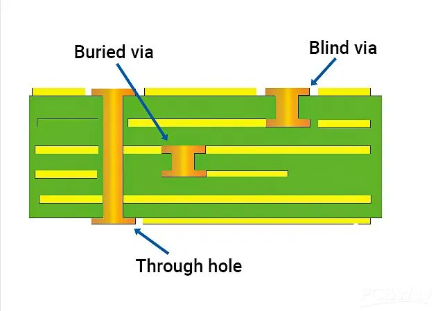
Buried vias are a type of via in a PCB that connects two or more internal layers without extending to the top or bottom surfaces. Unlike through-hole vias, which go all the way through the board, or blind vias, which connect an outer layer to an inner one, buried vias stay completely hidden within the board’s internal structure. This makes them a powerful tool for saving space on the outer layers, where components are typically placed.
Why are buried vias so important for compact electronics? They allow designers to pack more connections into a smaller area, which is critical for devices like smartphones, wearables, and IoT gadgets. By freeing up surface space, buried vias enable high-density PCB layouts, where components can be placed closer together. Additionally, they can reduce signal interference by shortening connection paths, which is vital for high-speed designs.
Buried Via PCB Design Rules: Getting the Basics Right
Designing with buried vias requires following specific rules to ensure manufacturability and reliability. Here are some essential buried via PCB design rules to keep in mind:
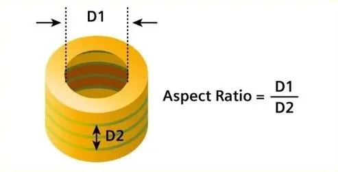
- Aspect Ratio: The aspect ratio of a buried via (depth to diameter) should typically be kept below 10:1. For example, if a via is 0.1 mm in diameter, its depth should not exceed 1 mm. This ensures proper plating during manufacturing and prevents defects.
- Minimum Size: Buried vias are often created using laser drilling, so their minimum diameter is usually around 0.1 mm to 0.15 mm. Check with your fabrication partner for exact limits, as smaller sizes may increase costs or risk reliability.
- Layer Alignment: Since buried vias are internal, precise layer alignment during PCB stackup is critical. Misalignment can lead to connection failures, so ensure your design software accounts for manufacturing tolerances, typically around ±0.05 mm.
- Spacing: Maintain adequate spacing between buried vias and other features like traces or pads to avoid shorts. A common guideline is to keep spacing at least 0.2 mm, though this varies based on board complexity.
Following these rules helps avoid costly redesigns and ensures your PCB performs as intended. Buried vias are often used in high-density interconnect (HDI) designs, where precision is non-negotiable.
High-Density PCB Layout: Maximizing Space Efficiency
High-density PCB layout is all about fitting more functionality into less space, and buried vias play a starring role. Here’s how to optimize your layout for compactness:
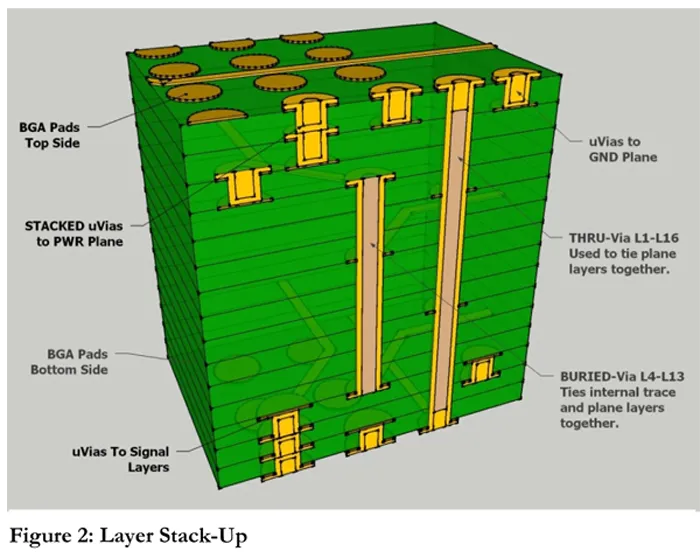
- Use Multi-Layer Boards: Buried vias shine in multi-layer PCBs (6 layers or more). They allow routing between internal layers, freeing up surface space for components. For instance, a 10-layer board might use buried vias between layers 3 and 6 to handle dense signal routing.
- Component Placement: Place high-pin-count components like microcontrollers or BGAs (Ball Grid Arrays) strategically. Use buried vias to route signals internally, reducing the need for long traces on the surface that can cause interference.
- Minimize Trace Lengths: Shorter traces reduce signal delay and noise. With buried vias, you can create direct connections between internal layers, cutting down trace lengths by up to 30% in some designs.
- Stack Vias if Needed: In ultra-dense designs, consider stacking buried vias with microvias (small vias connecting adjacent layers). This technique can further increase density but requires advanced manufacturing capabilities.
A well-planned high-density PCB layout not only saves space but also improves performance by reducing signal crosstalk and electromagnetic interference (EMI).
Buried Via Impedance Control: Ensuring Signal Integrity
Signal integrity is a major concern in high-speed electronics, and buried via impedance control is crucial for maintaining clean signals. Impedance mismatches can cause reflections, leading to data errors or signal loss. Here’s how to manage impedance with buried vias:
- Match Dielectric Properties: The dielectric constant (Dk) of the PCB material affects signal speed and impedance. For high-speed designs, use materials with a consistent Dk (e.g., 3.5 to 4.5 for FR-4) across layers to avoid mismatches at buried vias.
- Control Via Stub Lengths: A via stub is the unused portion of a via that can act as an antenna, causing signal reflections. Keep buried via stubs as short as possible—ideally less than 0.3 mm for signals above 1 GHz.
- Use Back-Drilling if Necessary: For critical high-speed signals, consider back-drilling to remove via stubs. While this is more common with through-hole vias, it can sometimes apply to buried vias in complex stackups.
- Simulate Impedance: Use PCB design software to simulate impedance before fabrication. Aim for a target impedance (e.g., 50 ohms for single-ended signals) and adjust via dimensions or layer spacing to match.
By focusing on buried via impedance control, you can ensure reliable performance in applications like USB-C, HDMI, or 5G devices where signal integrity is paramount.
PCB Miniaturization Techniques: Shrinking Without Sacrificing Performance
PCB miniaturization techniques are essential for modern electronics, where every millimeter counts. Buried vias are a cornerstone of miniaturization, but they’re just one part of the puzzle. Here are some proven strategies to shrink your PCB:
- Adopt HDI Technology: High-Density Interconnect (HDI) boards use buried and blind vias to achieve finer pitch routing. For example, HDI can reduce line widths to 0.075 mm and spacing to 0.05 mm, compared to 0.15 mm in standard PCBs.
- Opt for Smaller Components: Use surface-mount devices (SMDs) with smaller footprints, like 0201 or 01005 packages. Pair these with buried vias to route connections internally, avoiding crowded surface layers.
- Layer Stacking: Increase layer count while reducing board size. A 12-layer board with buried vias can handle the same complexity as a larger 4-layer board, cutting overall dimensions by 20-30%.
- Flexible PCBs: For ultra-compact designs, consider flexible or rigid-flex PCBs. Buried vias can still be used in these boards to save space, especially in wearable tech.
These PCB miniaturization techniques, combined with buried vias, allow you to design smaller, lighter devices without compromising on functionality.
Buried Via Stackup Design: Building a Solid Foundation
A well-thought-out buried via stackup design is the backbone of any high-density PCB. The stackup determines how layers are arranged, where vias are placed, and how signals and power are distributed. Here’s how to approach it:
- Plan Layer Assignment: Assign specific roles to each layer (e.g., signal, ground, power). Place high-speed signals on internal layers connected by buried vias to shield them from external noise.
- Balance Symmetry: Ensure the stackup is symmetrical to prevent warping during manufacturing. For an 8-layer board, pair buried vias between layers 2-3 and 6-7 to maintain balance.
- Ground Planes: Include dedicated ground planes near signal layers to reduce EMI. Buried vias can connect these planes internally, saving surface space.
- Thickness Control: Keep dielectric thickness consistent between layers with buried vias. Uneven thickness can affect impedance, so aim for uniformity (e.g., 0.2 mm per layer for standard HDI designs).
A robust buried via stackup design not only supports high-density layouts but also enhances thermal management and signal integrity.
Challenges and Solutions in Buried Via Design
While buried vias offer many benefits, they come with challenges. Understanding these hurdles and their solutions can save time and resources:
- Manufacturing Complexity: Buried vias require sequential lamination, a process where layers are bonded step by step. This increases costs by 15-25% compared to standard through-hole designs. Solution: Work closely with your fabrication partner to optimize the design for cost-effective production.
- Testing Limitations: Since buried vias are internal, they’re harder to test for defects. Solution: Use X-ray inspection during quality control to detect issues like voids or misalignments.
- Thermal Stress: Repeated heating and cooling during soldering can stress buried vias, risking cracks. Solution: Choose materials with a low coefficient of thermal expansion (CTE), such as high-Tg FR-4, to minimize stress.
By anticipating these challenges, you can design buried via PCBs that are both reliable and cost-efficient.
Practical Tips for Implementing Buried Vias
Ready to integrate buried vias into your next project? Here are some practical tips to get started:
- Start Small: If you’re new to buried vias, begin with a simpler design (e.g., a 6-layer board) before tackling complex HDI layouts.
- Use Design Software: Leverage advanced PCB design tools with built-in simulation for impedance and stackup. These can predict issues before manufacturing.
- Collaborate Early: Consult your fabrication team during the design phase to confirm buried via sizes, spacing, and stackup feasibility.
- Test Thoroughly: Perform signal integrity and thermal tests on prototypes to ensure buried vias perform as expected under real-world conditions.
Conclusion: Elevate Your Designs with Buried Vias
Buried vias are a game-changer for compact electronics, enabling high-density PCB layouts and supporting the miniaturization of modern devices. By mastering buried via PCB design rules, optimizing high-density layouts, controlling impedance, applying miniaturization techniques, and crafting effective stackup designs, you can unlock new levels of performance and efficiency in your projects.


