 ALLPCB


Are you facing challenges with PCB panelization, such as warping, component misalignment, or manufacturing defects? You're not alone. PCB panelization problems can delay production and increase costs, but they are often preventable with the right knowledge and techniques. In this comprehensive guide, we’ll dive into the most common issues like PCB panel warp, PCB depaneling issues, and PCB panel component misalignment, and provide practical solutions to help you achieve smoother manufacturing processes.
Whether you're a seasoned engineer or new to PCB design and manufacturing, this blog will walk you through troubleshooting steps and best practices to ensure high-quality results. Let’s explore how to tackle these challenges head-on!
What is PCB Panelization and Why Does It Matter?
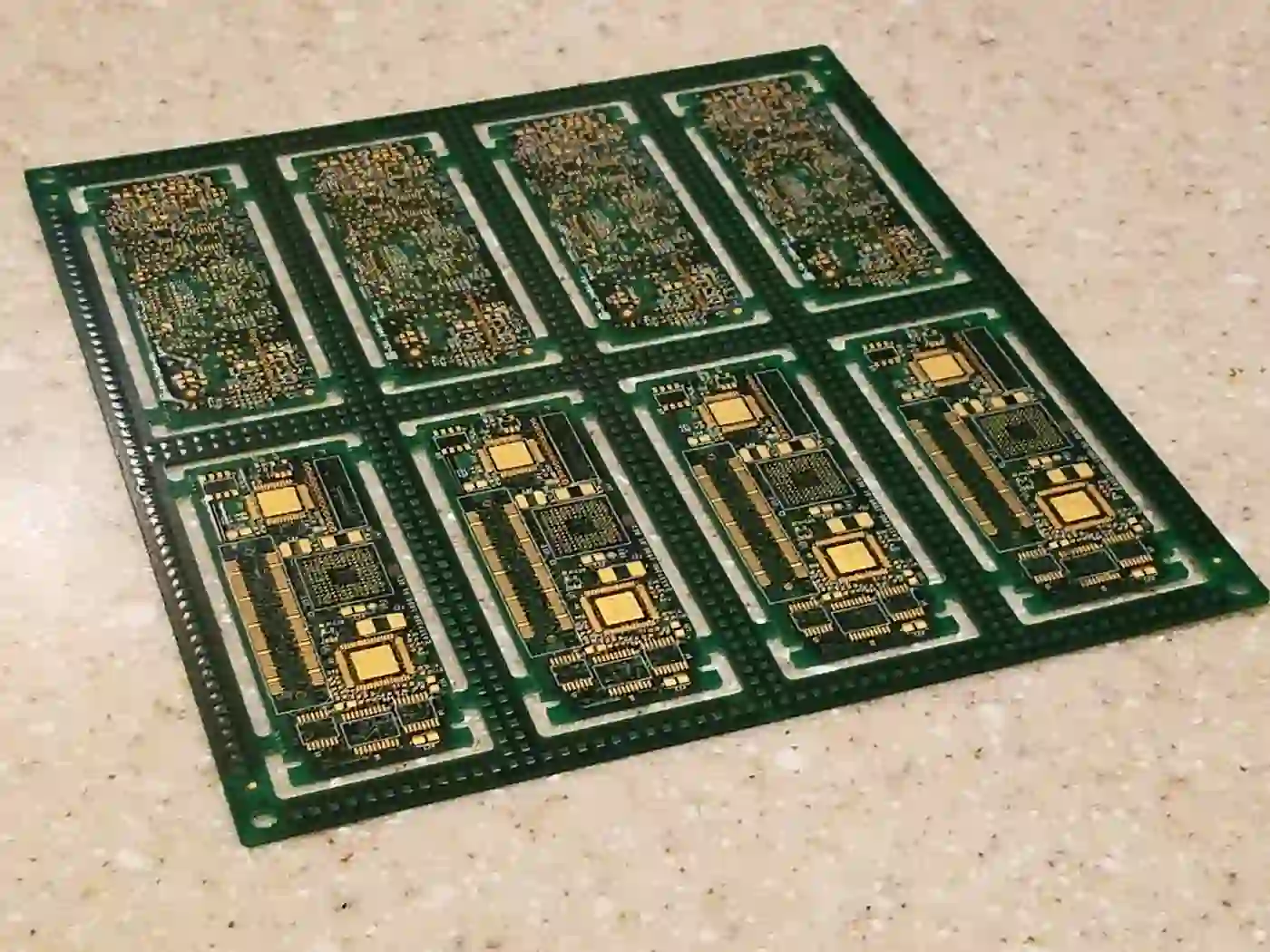
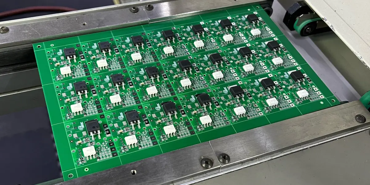
PCB panelization is the process of grouping multiple printed circuit boards (PCBs) into a single panel for efficient manufacturing. This technique reduces handling time, lowers production costs, and streamlines assembly by allowing multiple boards to be processed at once. However, when panelization isn’t done correctly, it can lead to a range of issues, from PCB panel manufacturing defects to delays in production.
Understanding the importance of proper panelization is the first step to avoiding common pitfalls. A well-designed panel ensures that boards remain intact during fabrication, assembly, and testing, while also making depaneling—the process of separating individual boards from the panel—easier and safer. Let’s break down the most frequent PCB panelization problems and how to solve them.
Common PCB Panelization Problems and Their Causes
Panelization issues can arise at various stages of the manufacturing process. Below, we’ve outlined the most common problems, including PCB panel warp, PCB depaneling issues, and PCB panel component misalignment, along with their root causes.
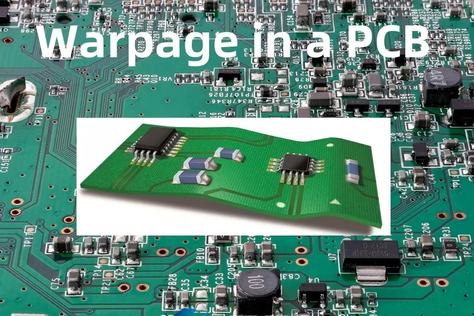
1. PCB Panel Warp
PCB panel warp refers to the bending or twisting of the panel during or after manufacturing. This issue can make assembly difficult and may even damage components or traces. Warping often occurs due to:
- Uneven Material Distribution: If the copper layers or substrate materials are not balanced across the panel, thermal expansion during soldering can cause uneven stress, leading to warping.
- Improper Panel Design: Large panels with insufficient support or poorly placed breakaway tabs can bend under their own weight or during handling.
- Thermal Stress: Exposure to high temperatures during reflow soldering (often exceeding 260°C for lead-free processes) can cause materials to expand or contract unevenly.
2. PCB Depaneling Issues
Depaneling is the process of separating individual PCBs from the panel after assembly. PCB depaneling issues, such as cracked boards or damaged components, often stem from:
- Poor Scoring or Routing Design: If V-grooves or mouse bites (small perforated holes) are not designed with the right depth or spacing, boards may not separate cleanly. For instance, a V-groove depth of less than 30% of the board thickness can lead to excessive stress during separation.
- Inadequate Tooling: Using dull or inappropriate depaneling tools can cause jagged edges or microcracks in the board.
- Component Proximity: Components placed too close to the panel edges (less than 5mm in some cases) can be damaged during depaneling.
3. PCB Panel Component Misalignment
Component misalignment during assembly on a panel can lead to soldering defects or non-functional boards. Common causes of PCB panel component misalignment include:
- Inaccurate Fiducial Marks: Fiducial marks are reference points used by assembly machines for alignment. If these marks are misplaced or unclear, pick-and-place machines may position components incorrectly, with errors as small as 0.1mm causing significant issues.
- Panel Flexing: If the panel warps or flexes during assembly, components may shift from their intended positions.
- Machine Calibration Errors: Automated assembly equipment must be precisely calibrated to account for panel dimensions and tolerances.
4. PCB Panel Manufacturing Defects
Manufacturing defects in PCB panels can include issues like delamination, broken traces, or incomplete etching. These problems often result from:
- Material Quality Issues: Low-quality substrates or laminates can lead to weak adhesion between layers, causing delamination under stress.
- Improper Handling: Rough handling during panelization or depaneling can cause physical damage, such as cracks or scratches.
- Design Flaws: Inadequate spacing between boards or insufficient edge clearance (e.g., less than 2mm) can result in manufacturing errors during cutting or drilling.
Solutions for PCB Panelization Problems
Now that we’ve identified the common issues, let’s explore actionable solutions to troubleshoot and prevent PCB panelization problems. These tips are designed to help you achieve reliable, high-quality results in your manufacturing process.
Solving PCB Panel Warp
To minimize or eliminate PCB panel warp, consider the following strategies:
- Balance Copper Distribution: Ensure that copper layers are evenly distributed across the panel. Use design software to check for imbalances and adjust trace layouts or add dummy copper fills if needed. Aim for a copper balance within 10% across layers.
- Use Support Structures: Add breakaway rails or tabs to provide extra support to large panels. A rail width of 5-10mm along the edges can significantly reduce bending.
- Control Thermal Exposure: Optimize reflow soldering profiles to minimize thermal stress. For example, limit peak temperatures to 245-260°C for lead-free soldering and ensure gradual cooling to prevent sudden contraction.
Addressing PCB Depaneling Issues
Preventing PCB depaneling issues requires careful planning in both design and execution:
- Optimize V-Grooves and Mouse Bites: Design V-grooves with a depth of 30-40% of the board thickness and a width of about 0.3mm for clean separation. For mouse bites, use a hole diameter of 0.8-1.2mm with 5-7 holes spaced evenly along the break line.
- Use Proper Tools: Invest in high-quality depaneling tools, such as precision routers or laser cutters, to ensure clean cuts without stressing the board.
- Protect Components: Maintain a minimum clearance of 5mm between components and panel edges to avoid damage during separation. If space is limited, consider using protective tape or fixtures during depaneling.
Correcting PCB Panel Component Misalignment
Ensuring accurate component placement on PCB panels involves attention to detail and proper setup:
- Verify Fiducial Marks: Place at least three fiducial marks on the panel, ideally near the corners, with a diameter of 1-2mm and a clear contrast against the background. Double-check their positions in the design files before fabrication.
- Minimize Panel Flexing: Use rigid materials for the panel and ensure proper clamping during assembly to prevent movement. A panel thickness of at least 1.6mm is recommended for most applications.
- Calibrate Equipment: Regularly calibrate pick-and-place machines to maintain placement accuracy within 0.05mm. Perform test runs on sample panels to confirm alignment before full production.
Preventing PCB Panel Manufacturing Defects
Reducing manufacturing defects starts with quality control and thoughtful design:
- Choose High-Quality Materials: Select reliable substrates and laminates with consistent properties. For example, FR-4 material with a glass transition temperature (Tg) of 130-140°C is suitable for most standard applications.
- Follow Design Guidelines: Maintain a minimum edge clearance of 2-3mm between individual boards on the panel to avoid cutting or drilling errors. Include clear markings for panel orientation to prevent handling mistakes.
- Implement Quality Checks: Conduct visual inspections and automated optical inspections (AOI) after each manufacturing stage to catch defects early. For instance, AOI can detect trace breaks or misaligned vias with an accuracy of up to 99.9%.
Best Practices for Successful PCB Panelization
Beyond troubleshooting specific issues, adopting best practices for PCB panelization can save time and resources in the long run. Here are some key tips to ensure a smooth process:
- Collaborate with Manufacturers Early: Share your panelization design files with your fabrication and assembly partners during the planning phase. They can provide feedback on panel size, tooling holes, and other specifications to avoid issues.
- Use Standard Panel Sizes: Stick to common panel dimensions, such as 18x24 inches or 9x12 inches, to match standard manufacturing equipment and reduce setup costs.
- Test Before Full Production: Create a small batch of panels for testing before scaling up. This allows you to identify potential problems like PCB panel warp or PCB panel component misalignment without risking a large order.
- Document Everything: Keep detailed records of your panelization designs, including tab placements, groove specifications, and material choices. This documentation can help troubleshoot recurring issues and improve future designs.
How to Choose the Right Panelization Method
There are several panelization methods, each suited to different project needs. Understanding these options can help you avoid common PCB panelization problems:
- Tab Routing with Breakaway Tabs: This method uses small tabs to hold boards together, which are broken off after assembly. It’s ideal for small to medium-sized boards but requires careful tab placement to avoid stress points.
- V-Groove Scoring: V-grooves are cut into the panel to create weak points for easy separation. This works well for rectangular boards and minimizes damage during depaneling if grooves are designed properly.
- Mouse Bites: Small perforated holes are used to connect boards, allowing for manual separation. This method is cost-effective for low-volume production but may not be suitable for delicate or high-density boards.
Conclusion: Mastering PCB Panelization for Better Results
PCB panelization is a critical step in the manufacturing process, but it comes with challenges like PCB panel warp, PCB depaneling issues, and PCB panel component misalignment. By understanding the causes of these common PCB panelization problems and applying the solutions and best practices outlined in this guide, you can significantly improve the quality and efficiency of your production runs.
From balancing copper distribution to optimizing V-grooves and ensuring accurate fiducial marks, every detail matters. Taking the time to design and test your panels carefully will help you avoid costly delays and achieve reliable, high-performing PCBs. With these strategies in hand, you’re well-equipped to tackle any PCB panel manufacturing defects and streamline your workflow.
Start implementing these tips in your next project and see the difference in your results. Remember, a little preparation goes a long way in ensuring smooth panelization and assembly processes!


