 ALLPCB


If you're dealing with plated through-hole (PTH) issues in your printed circuit board (PCB) designs, you're not alone. Common defects like PTH barrel cracks, plated through-hole voids, inner layer connection issues, inconsistent PTH plating thickness, and the need for effective PTH repair methods can impact the reliability and performance of your boards. In this practical guide, we'll dive deep into identifying, troubleshooting, and resolving these problems with actionable steps and detailed insights. Whether you're a seasoned engineer or new to PCB manufacturing, this blog will help you tackle PTH defects with confidence.
What Are Plated Through-Holes (PTH) and Why Do They Matter?
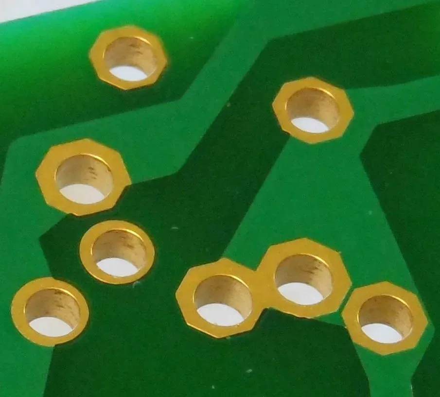
Plated through-holes are essential components of a PCB, creating conductive pathways between different layers of the board. These holes are drilled through the PCB and then plated with a layer of copper, typically around 20-25 micrometers thick, to ensure electrical connectivity. PTHs are critical for mounting through-hole components and enabling signals to pass between layers in multilayer boards.
However, defects in PTHs can lead to electrical failures, mechanical weaknesses, and reduced board lifespan. Issues like cracks in the copper barrel, voids in the plating, or poor inner layer connections can cause intermittent signals or complete circuit failure. Understanding and addressing these defects is vital for maintaining high-quality PCB performance, especially in demanding applications like automotive, aerospace, and telecommunications.
Common Plated Through-Hole Defects and Their Causes
Before diving into troubleshooting, let's explore the most common PTH defects, their root causes, and their impact on PCB functionality. By identifying the issue early, you can save time and resources during manufacturing and testing.
1. PTH Barrel Cracks
PTH barrel cracks refer to fractures or breaks in the copper plating inside the hole. These cracks often occur at the corners or along the barrel due to mechanical stress or thermal expansion during soldering or operation. For instance, a temperature increase from 25°C to 260°C during reflow soldering can cause the PCB material to expand, stressing the copper plating if the material's coefficient of thermal expansion (CTE) is mismatched.
Causes:
- Excessive thermal stress during soldering or operation.
- Poor drilling quality, leaving rough edges that weaken the copper plating.
- Insufficient copper thickness, often below the recommended 20 micrometers, reducing mechanical strength.
Impact: Barrel cracks can interrupt electrical connectivity, leading to signal loss or complete failure, especially in high-frequency applications where impedance control is critical (e.g., maintaining 50 ohms for RF signals).
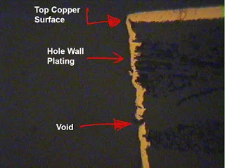
2. Plated Through-Hole Voids
Plated through-hole voids are areas within the PTH where copper plating is missing or incomplete. These voids often form during the electroplating process if air bubbles, contaminants, or uneven current distribution prevent uniform copper deposition.
Causes:
- Contamination in the plating bath, such as dust or organic residues.
- High aspect ratios (hole depth to diameter), like 10:1, making it hard for plating solution to reach the center of the hole.
- Inadequate cleaning of drilled holes before plating, leaving debris that blocks copper adhesion.
Impact: Voids reduce the conductive area, increasing resistance and potentially causing overheating or signal degradation. In severe cases, they can lead to open circuits.
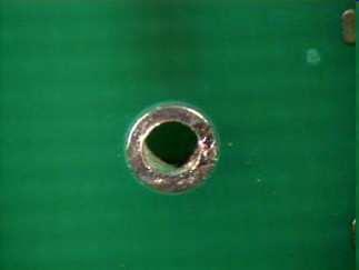
3. Inner Layer Connection Issues
Inner layer connection issues occur when the copper plating in the PTH fails to properly connect with the inner copper layers of a multilayer PCB. This defect often results in poor electrical conductivity between layers, disrupting signal paths.
Causes:
- Misalignment during drilling, preventing the hole from intersecting the inner layer copper accurately.
- Insufficient etching or cleaning, leaving oxide layers that block copper-to-copper bonding.
- Delamination of inner layers due to excessive heat or pressure during lamination, causing gaps.
Impact: These issues can lead to intermittent connections or total signal loss, especially in complex designs with high layer counts (e.g., 12-layer boards for advanced electronics).
4. Inconsistent PTH Plating Thickness
PTH plating thickness should ideally be uniform, with a minimum of 20 micrometers as per industry standards like IPC-6012. However, variations in thickness can occur, with some areas as thin as 10 micrometers or less, compromising reliability.
Causes:
- Uneven current distribution during electroplating, often due to poor bath agitation.
- High aspect ratio holes where plating solution struggles to penetrate evenly.
- Short plating times, reducing the overall copper deposit.
Impact: Thin plating reduces mechanical strength, making the PTH prone to cracking under stress. It also increases electrical resistance, affecting signal integrity in high-speed circuits (e.g., data rates above 10 Gbps).
Troubleshooting PTH Defects: Step-by-Step Solutions
Now that we've identified the common defects, let's walk through practical troubleshooting steps to diagnose and resolve these issues. These solutions are designed to help you pinpoint problems during design, manufacturing, or post-production stages.
Diagnosing PTH Barrel Cracks
Step 1: Visual and Microscopic Inspection
Use a high-magnification microscope (at least 50x) to inspect the PTH barrel for visible cracks. Cross-sectioning a sample board can reveal internal fractures not visible from the surface.
Step 2: Thermal Stress Testing
Subject the PCB to thermal cycling (e.g., -40°C to 85°C for 100 cycles) to simulate real-world conditions. Monitor for changes in electrical continuity using a multimeter to detect crack progression.
Solution:
- Optimize drilling parameters to ensure smooth hole walls, reducing stress points. For example, use a drill speed of 80,000 RPM with a feed rate of 100 inches per minute for FR-4 material.
- Choose PCB materials with a lower CTE (e.g., below 15 ppm/°C) to minimize thermal expansion mismatch.
- Increase copper plating thickness to at least 25 micrometers for better durability.
Addressing Plated Through-Hole Voids
Step 1: X-Ray Inspection
Use X-ray imaging to detect internal voids in the PTH plating without destructive testing. This method is particularly effective for high-density boards.
Step 2: Process Review
Examine the electroplating process logs for anomalies in current density (ideally 15-25 ASF, or amperes per square foot) or plating bath composition.
Solution:
- Implement thorough cleaning steps post-drilling, such as ultrasonic cleaning, to remove debris from holes.
- Adjust plating bath agitation to ensure uniform solution flow, especially for high aspect ratio holes (e.g., 8:1 or higher).
- Limit hole aspect ratios in design to 6:1 or lower to improve plating uniformity.
Fixing Inner Layer Connection Issues
Step 1: Continuity Testing
Use a netlist-based tester to check connectivity between PTHs and inner layers. A resistance reading above 10 milliohms may indicate a poor connection.
Step 2: Cross-Section Analysis
Cut a sample board to inspect the PTH alignment with inner layers under a microscope. Look for gaps or oxide buildup at the connection points.
Solution:
- Enhance drilling accuracy by using advanced CNC machines with a tolerance of ±0.002 inches.
- Apply a desmear process after drilling to remove resin smears and improve copper adhesion to inner layers.
- Control lamination temperatures (e.g., below 180°C for standard FR-4) to prevent delamination.
Ensuring Consistent PTH Plating Thickness
Step 1: Thickness Measurement
Use a microsectioning technique or eddy current testing to measure copper thickness at multiple points along the PTH barrel. Aim for a minimum of 20 micrometers per IPC standards.
Step 2: Plating Process Audit
Review the plating time and current settings. A plating time of 60-90 minutes at 20 ASF is typically sufficient for standard PTHs.
Solution:
- Extend plating duration if thickness is below specification, monitoring for over-plating risks.
- Use pulse plating techniques to improve copper distribution in high aspect ratio holes.
- Regularly maintain and filter plating baths to avoid contamination affecting deposition.
PTH Repair Methods for Damaged Holes
Sometimes, despite best efforts, PTHs get damaged during manufacturing or assembly. Repairing these holes is often more cost-effective than scrapping the board. Here are proven PTH repair methods to restore functionality.
Using Eyelets or Funnelets
Eyelets or funnelets are small metal inserts used to reinforce or repair damaged PTHs. They are pressed into the hole to create a new conductive path.
Process:
- Clean the damaged PTH to remove debris or old plating.
- Select an eyelet with a diameter matching the hole (e.g., 0.040 inches for a standard PTH).
- Insert and crimp the eyelet using a specialized tool to ensure a secure fit.
- Solder the eyelet to ensure electrical connectivity.
Best For: Boards with isolated PTH damage where full re-plating isn't feasible.
Re-Plating Damaged Holes
For boards with multiple damaged PTHs, re-plating the holes can be a viable solution. This involves stripping the old copper and applying a new layer.
Process:
- Strip existing copper using a chemical etchant, ensuring no residue remains.
- Re-drill if necessary to restore hole dimensions (e.g., to a tolerance of ±0.001 inches).
- Re-plate the holes using an electroplating setup, targeting 25 micrometers of copper thickness.
Best For: High-value boards where maintaining original design integrity is critical.
Preventing PTH Defects in Future Designs
Prevention is always better than repair. Incorporate these best practices into your PCB design and manufacturing process to minimize PTH defects.
- Design Considerations: Keep hole aspect ratios below 6:1 and avoid placing PTHs near high-stress areas like board edges.
- Material Selection: Opt for substrates with stable thermal properties (e.g., CTE of 12-15 ppm/°C) to reduce stress during temperature changes.
- Process Control: Implement strict quality checks during drilling, plating, and lamination to catch issues early.
- Testing: Use automated optical inspection (AOI) and X-ray systems to detect defects before assembly.
Conclusion
Troubleshooting common plated through-hole defects like PTH barrel cracks, plated through-hole voids, inner layer connection issues, and inconsistent PTH plating thickness doesn't have to be a daunting task. By understanding the root causes, employing systematic diagnostic techniques, and applying effective PTH repair methods, you can ensure the reliability and performance of your PCBs. Prevention through thoughtful design and stringent manufacturing controls will further reduce the likelihood of these issues, saving time and cost in the long run.
At ALLPCB, we're committed to supporting engineers with the tools and knowledge needed to achieve flawless PCB production. Whether you're tackling a complex multilayer design or a simple prototype, addressing PTH defects with precision is key to success. Keep this guide handy as a reference for your next project, and watch your board quality soar.


