 ALLPCB


If you're dealing with signal integrity issues in a 12-layer PCB, you're likely facing challenges like signal reflection, crosstalk, impedance mismatch, or signal loss. These problems can disrupt performance, especially in high-speed designs. The good news? They can be addressed with a structured troubleshooting approach. In this guide, we'll walk you through practical steps to identify and resolve these issues in 12-layer PCB designs, using simulation tools and real-world techniques tailored for complex multilayer boards.
Whether you're a seasoned engineer or tackling a high-density design for the first time, this blog will break down the causes of signal integrity problems and provide actionable solutions for 12-layer PCB signal integrity simulation, 12-layer PCB signal reflection, 12-layer PCB crosstalk, 12-layer PCB impedance mismatch, and 12-layer PCB signal loss. Let’s dive into the details to ensure your PCB performs at its best.
Understanding Signal Integrity in 12-Layer PCBs
A 12-layer PCB is often used in advanced applications like telecommunications, high-speed computing, and industrial systems. With multiple layers dedicated to power, ground, and signal routing, maintaining signal integrity becomes a complex task. Signal integrity refers to the quality of an electrical signal as it travels through the board. When issues arise, they can cause data errors, timing delays, or complete system failure.
Common signal integrity problems in 12-layer PCBs include:
- Signal Reflection: Occurs when a signal bounces back due to improper termination or impedance mismatch.
- Crosstalk: Interference between adjacent traces, especially in densely packed layers.
- Impedance Mismatch: Variations in trace impedance that distort signal transmission.
- Signal Loss: Degradation of signal strength due to dielectric losses or long trace lengths.
These issues are magnified in a 12-layer design due to the increased number of layers, tighter spacing, and higher signal speeds often exceeding 1 GHz. Solving them requires a mix of design foresight, simulation, and troubleshooting techniques.
Step 1: Identifying Signal Integrity Issues in 12-Layer PCBs
Before fixing a problem, you need to know what you're dealing with. Start by observing symptoms in your design. Are you seeing data corruption, unexpected delays, or erratic behavior in your system? These are telltale signs of signal integrity issues. Use the following methods to pinpoint the root cause:
- Oscilloscope Measurements: Connect an oscilloscope to critical nets to check for overshoot, undershoot, or ringing, which indicate 12-layer PCB signal reflection.
- Eye Diagram Analysis: For high-speed signals, an eye diagram can reveal timing jitter or signal degradation due to 12-layer PCB signal loss.
- Noise Monitoring: Use a spectrum analyzer to detect electromagnetic interference (EMI) or 12-layer PCB crosstalk between traces.
Once you've gathered data, compare it against your design specifications. For instance, if your signal rise time is slower than expected (e.g., above 500 ps for a 2.5 GHz signal), you might be dealing with signal loss or impedance mismatch.
Step 2: Common Causes of Signal Integrity Issues in 12-Layer PCBs
Understanding why these issues occur is key to preventing and fixing them. Here are the primary causes specific to a 12-layer PCB design:
1. Impedance Mismatch (12-Layer PCB Impedance Mismatch)
In a 12-layer PCB, maintaining consistent impedance (typically 50 ohms for high-speed signals) across all signal layers is challenging. Variations in trace width, dielectric thickness, or proximity to ground planes can cause mismatches. For example, if a trace on layer 3 is 5 mils wide but a similar trace on layer 9 is 6 mils due to manufacturing tolerances, impedance can vary by 10-15%, leading to reflections.
2. Signal Reflection (12-Layer PCB Signal Reflection)
Reflections happen when a signal encounters a sudden change in impedance, often at connectors or vias. In a 12-layer board, vias are unavoidable due to layer transitions, but a poorly designed via stub can act as a reflective stub, sending signals back along the trace.
3. Crosstalk (12-Layer PCB Crosstalk)
With multiple signal layers stacked closely together, crosstalk becomes a significant issue. If two high-speed traces on adjacent layers are routed in parallel for more than 100 mils without proper spacing (e.g., less than 3x the trace width), capacitive coupling can introduce noise, degrading signal quality.
4. Signal Loss (12-Layer PCB Signal Loss)
Signal loss in a 12-layer PCB often results from dielectric losses in the PCB material or long trace lengths. High-frequency signals (above 1 GHz) are particularly vulnerable, as energy dissipates into the substrate. For instance, using a standard FR-4 material with a dissipation factor of 0.02 can cause significant loss compared to low-loss materials with a factor of 0.002.
Step 3: Practical Troubleshooting Techniques for 12-Layer PCBs
Now that you’ve identified potential issues and their causes, let’s explore hands-on solutions to troubleshoot and resolve them. These methods are tailored for the complexity of a 12-layer PCB design.
1. Use Simulation Tools for Diagnosis (12-Layer PCB Signal Integrity Simulation)
Simulation is a powerful way to predict and troubleshoot signal integrity issues before manufacturing. Tools for 12-layer PCB signal integrity simulation can model impedance, reflections, and crosstalk. Follow these steps:
- Import your PCB layout into a simulation tool.
- Set up parameters like signal frequency (e.g., 2.5 GHz), trace geometry, and material properties (dielectric constant of 4.2 for FR-4).
- Run a time-domain reflectometry (TDR) simulation to identify impedance mismatches. Look for spikes in the TDR plot indicating reflection points.
- Simulate crosstalk by analyzing coupling between adjacent traces. Aim for a crosstalk voltage below 5% of the signal amplitude (e.g., less than 50 mV for a 1V signal).
Simulation saves time by catching issues early, reducing the need for costly prototypes.
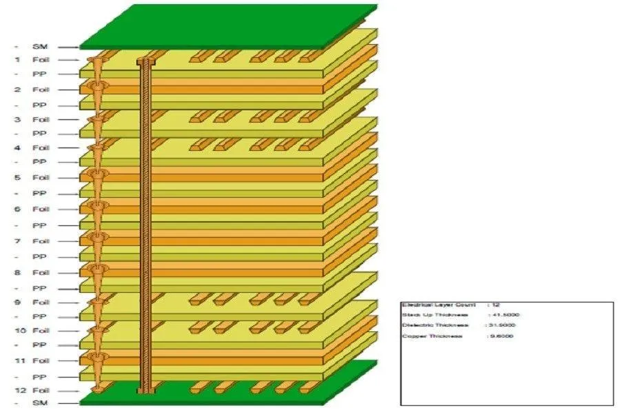
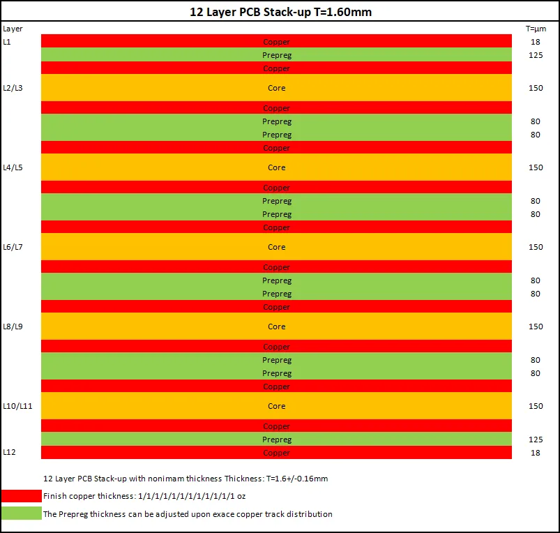
2. Optimize Layer Stack-Up Design
A well-planned stack-up minimizes signal integrity issues. In a 12-layer PCB, dedicate multiple layers to ground and power planes to provide a stable reference for signals. A typical stack-up might look like this:
- Layer 1: Top Signal
- Layer 2: Ground
- Layer 3: Signal
- Layer 4: Power
- Layer 5: Ground
- Layer 6: Signal
- (Continue alternating signal, ground, and power layers)
Placing ground planes adjacent to signal layers reduces crosstalk and ensures consistent impedance. Maintain symmetry in the stack-up to avoid warping during manufacturing.
3. Address Impedance Mismatch
For 12-layer PCB impedance mismatch, calculate the required trace width and spacing using an impedance calculator based on your material’s dielectric constant (e.g., 4.2 for FR-4) and layer thickness (e.g., 1.6 mm total board thickness). If mismatches persist, consider adding series termination resistors (e.g., 33 ohms) near the driver to dampen reflections.
4. Mitigate Signal Reflection
To tackle 12-layer PCB signal reflection, minimize via stubs by back-drilling or using blind vias in your design. Ensure proper termination by matching the load impedance to the trace impedance. For example, a 50-ohm trace should connect to a 50-ohm load to prevent reflections.
5. Reduce Crosstalk
For 12-layer PCB crosstalk, increase spacing between high-speed traces to at least 3x the trace width. If space is limited, route critical signals on different layers with a ground plane in between to act as a shield. Keep parallel trace lengths short to limit coupling.
6. Minimize Signal Loss
To combat 12-layer PCB signal loss, use low-loss dielectric materials for high-frequency designs. Shorten trace lengths where possible, and avoid routing high-speed signals across split planes, as this introduces discontinuities that degrade the signal.
Step 4: Testing and Validation After Fixes
After applying these solutions, validate your design to ensure the issues are resolved. Re-run oscilloscope tests and eye diagram analyses to confirm signal quality. For instance, check if the signal overshoot is below 10% of the peak voltage (e.g., less than 100 mV for a 1V signal). If problems persist, revisit the simulation to identify overlooked factors like via inductance or parasitic capacitance.
Additionally, perform environmental testing to simulate real-world conditions. Temperature variations or humidity can affect dielectric properties, so test your PCB across a range of conditions (e.g., 0°C to 70°C) to ensure reliability.
Step 5: Best Practices for Preventing Future Issues
Troubleshooting is essential, but prevention is even better. Adopt these best practices during the design phase of your 12-layer PCB to minimize signal integrity issues:
- Plan your layer stack-up early, prioritizing ground and power planes near signal layers.
- Use controlled impedance routing for all high-speed signals, maintaining consistent trace widths (e.g., 5 mils for 50-ohm impedance on FR-4).
- Avoid routing high-speed traces near board edges or over split planes.
- Incorporate decoupling capacitors (e.g., 0.1 μF) near power pins to stabilize voltage and reduce noise.
- Collaborate with your PCB manufacturer to ensure tight tolerances on trace widths and dielectric thickness.
Conclusion: Mastering Signal Integrity in 12-Layer PCBs
Troubleshooting signal integrity issues in a 12-layer PCB doesn’t have to be overwhelming. By following a systematic approach—identifying symptoms, understanding causes, using 12-layer PCB signal integrity simulation, and applying targeted fixes—you can resolve challenges like 12-layer PCB signal reflection, 12-layer PCB crosstalk, 12-layer PCB impedance mismatch, and 12-layer PCB signal loss. With the right tools and best practices, your high-speed designs can achieve optimal performance and reliability.
Start with simulation to catch issues early, optimize your layer stack-up, and validate every fix with thorough testing. By building prevention into your design process, you’ll save time and resources on future projects. A well-designed 12-layer PCB isn’t just a board—it’s the backbone of a high-performing system.


