 ALLPCB


If you're looking for a comprehensive resource on rigid-flex PCB stackups, you've come to the right place. This guide answers your core needs by diving deep into the essentials of rigid-flex PCB materials, manufacturing processes, assembly techniques, design rules, and cost optimization strategies. Whether you're an engineer designing complex electronics or a project manager seeking efficient solutions, you'll find actionable insights to streamline your next project. Let's explore everything you need to know about rigid-flex PCBs in detail.
What Are Rigid-Flex PCBs and Why Use Them?
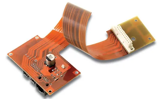
Rigid-flex PCBs combine the stability of rigid circuit boards with the adaptability of flexible circuits, making them ideal for modern electronics where space and durability are critical. These hybrid boards consist of rigid sections for mounting components and flexible sections for bending or folding, allowing for compact designs in devices like smartphones, medical equipment, and aerospace systems.
The primary advantage of rigid-flex PCBs is their ability to reduce the need for connectors and cables, which minimizes points of failure and enhances reliability. They also save space, reduce weight, and can withstand harsh environments due to their robust construction. Understanding their stackup—the arrangement of layers and materials—is the foundation for leveraging these benefits in your designs.
Understanding Rigid-Flex PCB Stackups
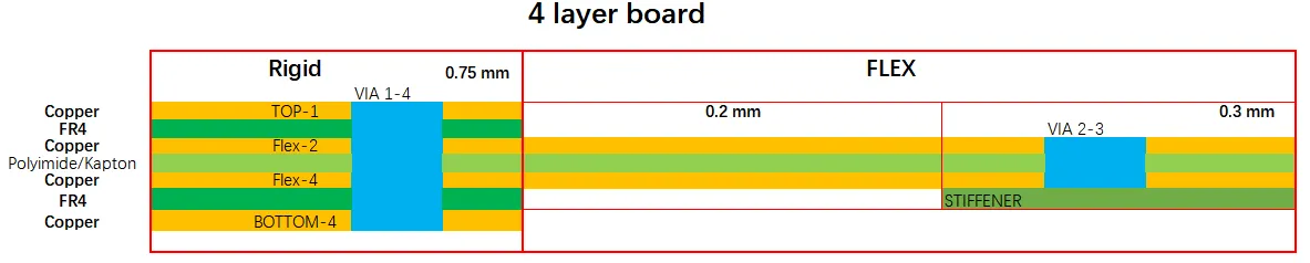
A rigid-flex PCB stackup refers to the layered structure of materials that make up the board, including conductive layers, insulating materials, and adhesive or bonding layers. A typical stackup might include rigid layers (often made of FR-4) for structural support and flexible layers (commonly polyimide) for bendability, bonded together in a specific configuration.
For example, a common 4-layer rigid-flex stackup might consist of two rigid layers sandwiching two flexible layers, with copper traces on each layer for signal routing. The arrangement must balance electrical performance, mechanical strength, and flexibility. Proper stackup design ensures signal integrity, with controlled impedance often targeted at 50 ohms for high-speed signals, and minimizes issues like crosstalk or signal loss.
Rigid-Flex PCB Materials: Choosing the Right Components
The choice of materials in rigid-flex PCB stackups directly impacts performance, durability, and cost. Let's break down the key materials used and their properties to help you make informed decisions for your projects.
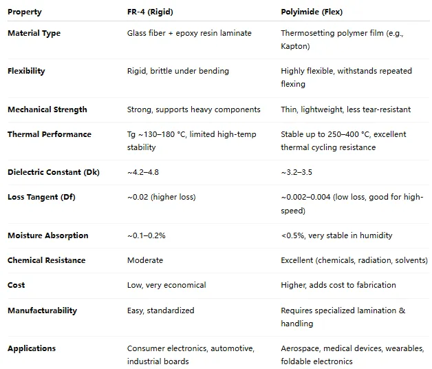
Rigid Materials
Rigid sections are typically made from FR-4, a glass-reinforced epoxy laminate known for its strength and thermal stability. FR-4 has a dielectric constant of around 4.5, making it suitable for many applications. For high-frequency designs, materials like Rogers laminates with lower dielectric constants (around 3.0) may be used to reduce signal loss.
Flexible Materials
Flexible layers are often made from polyimide, a material prized for its high tensile strength and ability to withstand repeated bending. Polyimide can endure temperatures up to 260°C, ideal for demanding environments. Some designs use adhesive-less polyimide to reduce thickness and improve flexibility, which is a critical consideration for tight bends.
Adhesives and Bonding
Adhesives bond rigid and flexible layers together. Acrylic or epoxy-based adhesives are common, though adhesive-less constructions are gaining popularity for better thermal performance and thinner profiles. The choice depends on the thermal and mechanical stresses your board will face.
The Rigid-Flex Manufacturing Process: Step by Step
Understanding the rigid-flex manufacturing process is crucial for ensuring your design translates into a functional product. Here's a detailed look at how these boards are made.
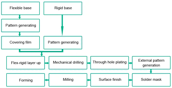
1. Design and Layer Planning
The process begins with creating a detailed stackup design, specifying the number of layers, material types, and thickness. For instance, a typical flex layer might be 0.002 inches thick, while rigid sections could be 0.062 inches. Designers use software to simulate signal integrity and mechanical stress before finalizing the layout.
2. Material Preparation
Raw materials are cut and prepared. Rigid materials like FR-4 are laminated with copper foil, while flexible polyimide layers are processed to ensure uniform thickness. Prepreg (pre-impregnated resin) layers are added for bonding during lamination.
3. Lamination
Layers are stacked and bonded under high pressure and temperature (often around 180°C) in a lamination press. This step ensures the rigid and flexible sections are securely joined without delamination, a common issue if temperatures or pressures are uneven.
4. Drilling and Plating
Holes are drilled for vias and component mounting. These holes are then plated with copper to create electrical connections between layers. For high-density designs, microvias (diameters as small as 0.006 inches) may be used to save space.
5. Etching and Patterning
Copper layers are etched to form the desired circuit patterns. Photolithography exposes the copper to UV light through a mask, defining traces as narrow as 0.003 inches for fine-pitch designs.
6. Final Assembly and Testing
After adding surface finishes like ENIG (Electroless Nickel Immersion Gold) for corrosion resistance, the boards undergo electrical testing to verify continuity and insulation resistance. Bend tests ensure flexible sections can withstand specified cycles, often up to 100,000 bends for dynamic applications.
Rigid-Flex Assembly: Key Considerations
Assembling rigid-flex PCBs requires special attention due to their hybrid nature. Here are the critical factors to keep in mind during the assembly phase.
Component Placement
Components are typically mounted on rigid sections for stability. Surface-mount technology (SMT) is commonly used, with placement accuracy within 0.001 inches to ensure proper alignment. Avoid placing heavy components near flexible areas to prevent stress during bending.
Stiffeners and Support
Stiffeners, often made of FR-4 or polyimide, are added to flexible sections near connectors or high-stress areas to prevent tearing. These can increase board thickness by 0.010 inches but are essential for durability.
Soldering Techniques
Reflow soldering is standard for rigid-flex assembly, with peak temperatures around 245°C for lead-free solder. Care must be taken to avoid thermal shock to flexible materials, which can warp or delaminate if overheated.
Rigid-Flex PCB Design Rules: Best Practices for Success
Designing a rigid-flex PCB requires adherence to specific rules to ensure functionality and manufacturability. Below are key guidelines to follow.
Layer Transitions
Minimize the number of layer transitions between rigid and flex sections to reduce stress. Use gradual transitions with a bend radius at least 10 times the thickness of the flex layer (e.g., 0.020 inches for a 0.002-inch layer) to prevent cracking.
Trace Routing
Route traces perpendicular to the bend line in flexible areas to avoid stress concentration. Maintain trace widths of at least 0.005 inches and spacing of 0.006 inches to ensure reliability during bending.
Via Placement
Avoid placing vias in bend areas, as they can crack under stress. Use teardrop-shaped vias near pads to reduce stress points, and ensure annular rings are at least 0.010 inches for stability.
Controlled Impedance
For high-speed signals, maintain controlled impedance (e.g., 50 ohms for single-ended signals) by adjusting trace width and dielectric thickness. Use simulation tools to verify impedance before manufacturing.
Rigid-Flex Stackup Cost Optimization: Balancing Quality and Budget
Cost is a significant factor in rigid-flex PCB projects. Here are proven strategies to optimize costs without compromising quality.
Simplify Stackup Design
Reduce the number of layers where possible. A 4-layer stackup is often more cost-effective than a 6-layer one, saving up to 20% on material and fabrication costs, depending on complexity.
Material Selection
Opt for standard materials like FR-4 and polyimide over exotic laminates unless high-frequency performance is critical. Standard materials can reduce costs by 15-30% compared to specialized options.
Panel Utilization
Design boards to maximize panel utilization during manufacturing. Efficient nesting can lower fabrication costs by up to 10%, as it reduces material waste.
Early Collaboration
Work closely with your manufacturer during the design phase to identify potential cost drivers, such as tight tolerances (e.g., below 0.005 inches for traces), which can increase production time and expense.
Common Challenges and How to Overcome Them
Rigid-flex PCBs present unique challenges due to their hybrid nature. Here are some common issues and solutions.
Delamination
Delamination between rigid and flex layers can occur due to thermal stress. Use compatible materials with similar coefficients of thermal expansion (CTE), and avoid excessive heat during assembly.
Signal Integrity Issues
High-speed signals can suffer from loss or crosstalk in flex areas. Maintain consistent dielectric thickness (e.g., 0.003 inches) and use ground planes to shield critical traces.
Mechanical Stress
Repeated bending can cause cracks or fatigue. Design with larger bend radii and reinforce high-stress areas with stiffeners to extend the board's lifespan.
Conclusion: Mastering Rigid-Flex PCB Stackups
Rigid-flex PCBs offer unparalleled advantages for compact, reliable electronics, but their success hinges on careful design and manufacturing. By understanding rigid-flex PCB materials, following a precise manufacturing process, adhering to assembly best practices, applying design rules, and optimizing costs, you can create high-performing boards tailored to your needs. This guide has provided the foundation to navigate these complexities, ensuring your next project is both innovative and efficient.
With the right approach, rigid-flex stackups can transform your designs, delivering durability and performance in even the most demanding applications. Keep these best practices in mind, and you'll be well-equipped to tackle any rigid-flex challenge.


