 ALLPCB


If you're searching for the best PCB design software with buried via support, you've come to the right place. Buried vias are critical for high-density interconnect (HDI) designs, allowing connections between inner layers of a printed circuit board (PCB) without affecting the outer layers. In this guide, we'll explore the features and functionality of buried via design tools, focusing on popular software options like Altium Designer, Eagle PCB, and KiCad. We'll cover how these tools handle buried vias, their key features, and how they can help you achieve precise and efficient PCB layouts for complex projects.
This comprehensive blog post will dive deep into buried via technology, the importance of software support for such designs, and a detailed breakdown of tools that cater to these needs. Whether you're an experienced engineer or just starting with HDI designs, this guide will provide actionable insights to enhance your workflow.
What Are Buried Vias and Why Are They Important in PCB Design?
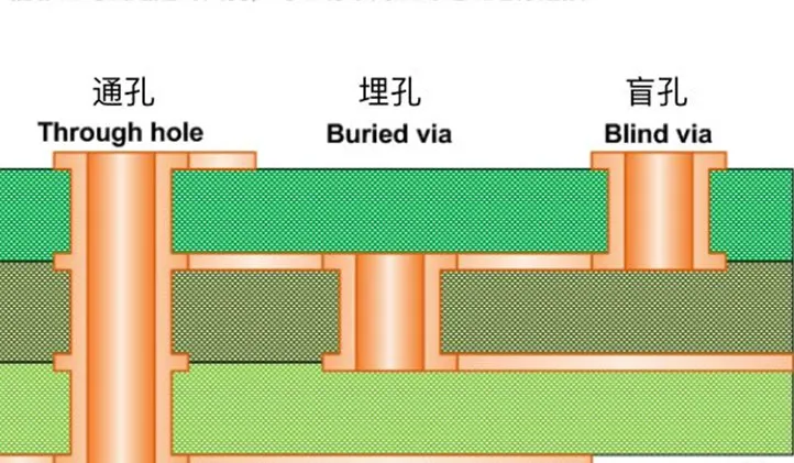
Buried vias are a type of via that connects internal layers of a multilayer PCB without extending to the outer layers. Unlike through-hole vias that span the entire board or blind vias that connect an outer layer to an inner one, buried vias remain hidden within the board's internal structure. This makes them ideal for high-density designs where space on the outer layers is limited, and signal integrity is paramount.
In modern electronics, buried vias are essential for reducing signal interference and improving performance in compact devices. For example, in a 6-layer PCB, buried vias might connect layers 2 through 5 to route high-speed signals at speeds up to 5 Gbps, avoiding crosstalk on the surface layers. They also help lower electromagnetic interference (EMI) by keeping sensitive traces away from external components. However, designing with buried vias requires specialized software capable of defining layer-specific connections and ensuring manufacturing accuracy.
Key Features to Look for in Buried Via Design Software
Not all PCB design tools support buried vias, and even among those that do, the functionality can vary widely. When choosing software for buried via design, consider the following features to ensure it meets your project needs:
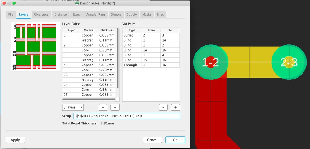
- Layer Stack Management: The software must allow precise control over layer stacks, enabling you to define which layers a via connects. This is critical for buried vias, as they must start and stop at specific internal layers.
- Via Type Customization: Look for tools that let you specify via types (buried, blind, through-hole) and set parameters like diameter and depth. For instance, a buried via might have a diameter of 0.2 mm to fit tight spacing in HDI designs.
- Design Rule Checking (DRC): Robust DRC features ensure that buried vias comply with manufacturing constraints, such as minimum spacing of 0.15 mm between vias or traces, preventing errors during fabrication.
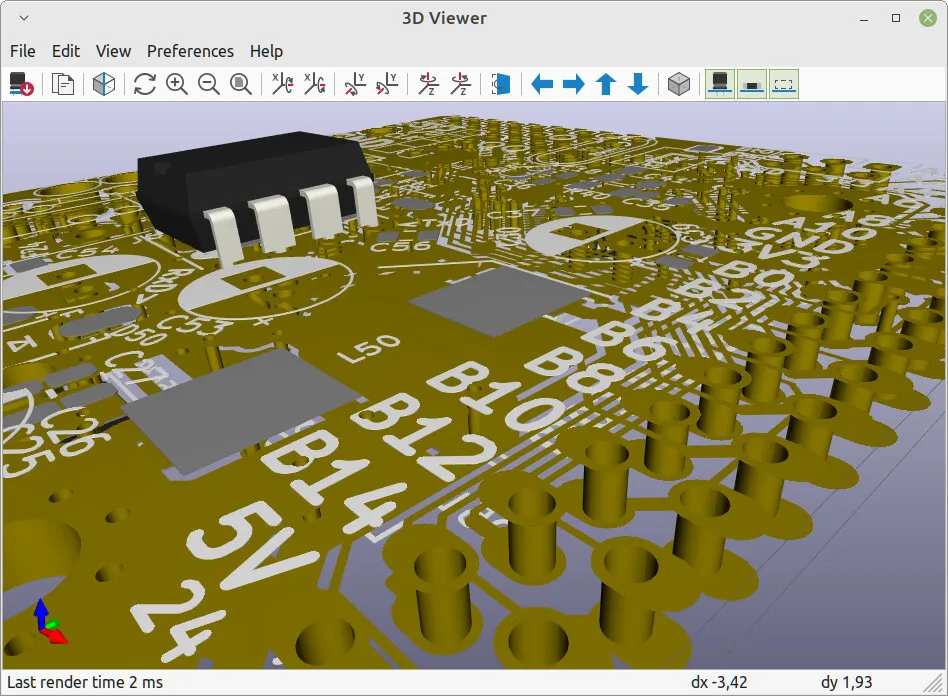
- 3D Visualization: A 3D view of the PCB helps verify the placement and depth of buried vias, ensuring they align correctly within the internal layers.
- Signal Integrity Analysis: For high-speed designs, software should simulate signal behavior, accounting for impedance mismatches (e.g., maintaining 50 ohms for controlled impedance lines) caused by buried vias.
- Manufacturing Output Support: The tool should generate accurate Gerber files and drill data that clearly communicate buried via specifications to fabricators.
These features collectively ensure that your buried via designs are both functional and manufacturable, saving time and reducing costly revisions.
Popular PCB Design Software with Buried Via Support
Let's explore some widely used PCB design tools that offer buried via support. We'll focus on their capabilities, ease of use, and specific functionalities related to buried via design.
Altium Designer: Advanced Buried Via Capabilities
Altium Designer is a leading choice for professional engineers working on complex multilayer boards. It offers robust support for buried vias, making it a go-to option for HDI designs. Here's how it excels:
- Layer Stack Manager: Altium allows you to define detailed layer stacks and assign buried vias to specific layer pairs. For example, you can create a via connecting layer 3 to layer 6 in an 8-layer board with just a few clicks.
- Via Configuration: You can customize via properties, such as setting a buried via depth to span only 0.5 mm of board thickness, ensuring precision in dense layouts.
- Rules-Driven Design: Altium's constraint manager lets you set clearance rules (e.g., 0.2 mm spacing between buried vias) to avoid manufacturing issues.
- Signal Integrity Tools: Built-in simulation helps analyze how buried vias affect high-speed signals, maintaining impedance control within ±10% of target values like 50 ohms.
- 3D Visualization: Its 3D rendering feature lets you inspect buried vias within the board structure, reducing the risk of misalignment.
Altium Designer is ideal for projects where buried vias are critical to performance, such as in telecommunications or aerospace applications. However, its advanced features come with a steeper learning curve and higher cost, which may not suit hobbyists or small-scale projects.
Eagle PCB: Buried Via Support for Mid-Level Designs
Eagle PCB is another popular tool, often favored by small teams and independent designers for its balance of functionality and affordability. Its support for buried vias is suitable for moderately complex designs. Key features include:
- Layer Pair Definition: Eagle lets you define buried vias by specifying start and stop layers, such as connecting layer 2 to layer 4 in a 6-layer PCB.
- Via Placement: You can manually place buried vias or use autorouting features, though customization options are less extensive than in premium tools.
- Design Rules: Eagle's DRC checks for via spacing and manufacturability, ensuring buried vias meet basic requirements like 0.3 mm clearance.
- Visualization: While Eagle offers a basic 3D view, it’s not as detailed as some competitors, which might limit verification of buried via placement.
Eagle PCB is a good fit for mid-range projects where buried vias are needed but the design complexity doesn’t demand top-tier simulation or visualization. It’s more accessible for those on a budget but may lack the depth required for cutting-edge HDI boards.
KiCad: Open-Source Buried Via Design Tool
KiCad is a free, open-source PCB design software that has gained popularity among hobbyists and professionals alike. While it’s not as feature-rich as paid alternatives, it does offer buried via support for cost-conscious designers. Here’s what it brings to the table:
- Layer Stack Control: KiCad allows you to define buried vias by setting layer connections, though the process can be less intuitive compared to premium tools.
- Via Settings: You can adjust via parameters like diameter (e.g., 0.25 mm for buried vias) to suit HDI layouts, though advanced customization is limited.
- DRC Features: KiCad includes design rule checks to flag issues with buried via spacing or alignment, helping maintain manufacturability.
- 3D Viewer: Its 3D visualization tool lets you see buried vias within the board, though rendering quality is basic.
- Community Support: Being open-source, KiCad benefits from an active user community that often develops plugins, such as via stitching tools, to enhance functionality.
KiCad is a fantastic option for those starting with buried via designs or working on a tight budget. While it may not match the advanced signal integrity analysis of other tools, it’s continuously improving and sufficient for many small to medium projects.
Comparing Buried Via Design Tools: Which One Suits Your Needs?
Choosing the right buried via design software depends on your project requirements, budget, and skill level. Here’s a quick comparison to help you decide:
| Software | Buried Via Support | Ease of Use | Advanced Features | Cost | Best For |
|---|---|---|---|---|---|
| Altium Designer | Excellent | Moderate | Signal integrity, 3D view | High | Professional HDI designs |
| Eagle PCB | Good | Easy | Basic DRC, limited 3D | Moderate | Mid-range projects |
| KiCad | Basic | Moderate | Community plugins, basic 3D | Free | Hobbyists, small projects |
For high-speed, high-density designs requiring buried vias to manage signals at frequencies above 1 GHz, a tool like Altium Designer is worth the investment. For simpler multilayer boards or budget constraints, Eagle PCB or KiCad can still deliver reliable results with buried via support.
Best Practices for Designing with Buried Vias
Regardless of the software you choose, following best practices ensures your buried via designs are effective and manufacturable. Here are some tips to keep in mind:
- Plan Layer Stacks Early: Define your layer stack before placing buried vias to avoid alignment issues. For instance, in a 10-layer board, decide which layers (e.g., 4 to 7) will use buried vias for signal routing.
- Minimize Via Count: Use buried vias only where necessary to reduce manufacturing costs, as they are more expensive to fabricate than through-hole vias.
- Check Manufacturer Capabilities: Ensure your fabricator supports buried vias with your specified dimensions, such as a minimum diameter of 0.15 mm, to avoid production delays.
- Optimize for Signal Integrity: Place buried vias strategically to shorten trace lengths and maintain impedance, targeting values like 50 ohms for high-speed lines.
- Validate with DRC: Always run design rule checks to catch errors in via spacing or layer connections before finalizing your design.
By adhering to these practices, you can leverage buried via design tools to create reliable, high-performance PCBs tailored to your project’s needs.
Challenges in Buried Via Design and How Software Helps
Designing with buried vias presents unique challenges, from increased fabrication costs to potential signal integrity issues. Here’s how software addresses these hurdles:
- Manufacturing Complexity: Buried vias require precise drilling and plating processes. Software with detailed output files ensures fabricators receive clear instructions, reducing errors.
- Signal Loss: At high frequencies (e.g., 10 GHz), buried vias can introduce signal loss. Advanced tools offer simulation features to predict and mitigate these effects.
- Cost Management: By visualizing via placement in 3D, software helps minimize the number of buried vias, keeping costs down while maintaining design integrity.
With the right buried via design software, you can navigate these challenges effectively, ensuring your PCB meets both performance and budget goals.
Conclusion: Choosing the Right Buried Via Design Tool
Buried vias are a powerful solution for creating compact, high-performance PCBs, but they demand specialized software to design effectively. Whether you opt for the advanced capabilities of Altium Designer, the balanced approach of Eagle PCB, or the cost-effective open-source option of KiCad, each tool offers unique strengths for buried via support. Consider your project’s complexity, budget, and specific requirements when selecting the best buried via design tool for your needs.
At ALLPCB, we understand the importance of precision in HDI designs. By pairing the right software with our manufacturing expertise, you can bring your buried via projects to life with confidence. Explore these tools, apply the best practices shared in this guide, and elevate your PCB designs to the next level.


