 ALLPCB


When it comes to assembling printed circuit boards (PCBs) for space probes, precision and reliability are non-negotiable. Space probe PCB soldering techniques must ensure that every connection withstands the extreme conditions of space, from intense vibrations during launch to temperature swings of -150°C to +150°C in orbit. Solder joint reliability in space is critical to mission success, as even a single failure can jeopardize years of planning and investment. At ALLPCB, we understand the unique challenges of PCB assembly for extreme environments, and in this blog, we’ll share best practices for high-reliability soldering, including the role of conformal coating for space probe PCBs. Whether you’re an engineer designing for a satellite or a deep-space mission, this guide will provide actionable insights to ensure your assemblies perform flawlessly.
Why High-Reliability Soldering Matters for Space Probe PCBs
Space is an unforgiving environment. PCBs in space probes face challenges unlike those in terrestrial applications. During launch, components endure vibrations that can reach 10-20 g-force, risking solder joint cracks if not executed with precision. In orbit, thermal cycling—rapid shifts between extreme cold and heat—can cause expansion and contraction, stressing connections. Cosmic radiation can also degrade materials over time, while the vacuum of space prevents heat dissipation through convection, pushing components to their thermal limits.
High-reliability soldering is the foundation of a space probe’s electronic systems. A single failed solder joint can disrupt communication, navigation, or data collection, potentially ending a mission. By following best practices for PCB assembly in extreme environments, engineers can minimize risks and ensure long-term performance.

Key Challenges in Space Probe PCB Soldering
Before diving into best practices, let’s outline the specific challenges that make soldering for space probes so demanding:
- Vibration and Mechanical Stress: Launch vibrations and micro-meteorite impacts can weaken solder joints if not properly designed or executed.
- Thermal Extremes: Temperature fluctuations in space can range from -150°C near shadowed areas to +150°C in direct sunlight, causing material fatigue over time.
- Radiation Exposure: High-energy particles can degrade solder materials and PCB substrates, leading to potential failures.
- Vacuum Conditions: The lack of atmosphere means outgassing from materials can contaminate nearby components, and there’s no air to dissipate heat.
- Long Mission Durations: Space probes often operate for decades, requiring solder joints to maintain integrity without maintenance or repair.
Addressing these challenges starts with meticulous soldering techniques tailored for space applications. Let’s explore the best practices to achieve solder joint reliability in space.
Best Practices for Space Probe PCB Soldering Techniques
1. Select the Right Solder Materials
Choosing the correct solder alloy is the first step in ensuring reliability. For space applications, lead-based solders like Sn63Pb37 (63% tin, 37% lead) are often preferred over lead-free alternatives due to their proven track record in high-reliability environments. Lead-based solders have a lower melting point (around 183°C) compared to lead-free options (often above 217°C), reducing thermal stress on components during assembly. They also exhibit better resistance to tin whisker growth, a phenomenon where thin metal filaments form and cause short circuits—a significant concern in the vacuum of space.
Additionally, flux selection is critical. Use no-clean or water-soluble fluxes that minimize residue, as residues can outgas in a vacuum, leading to contamination. Ensure compliance with standards like NASA-STD-8739.3, which governs soldering for spaceflight hardware.
2. Optimize Solder Joint Design for Reliability
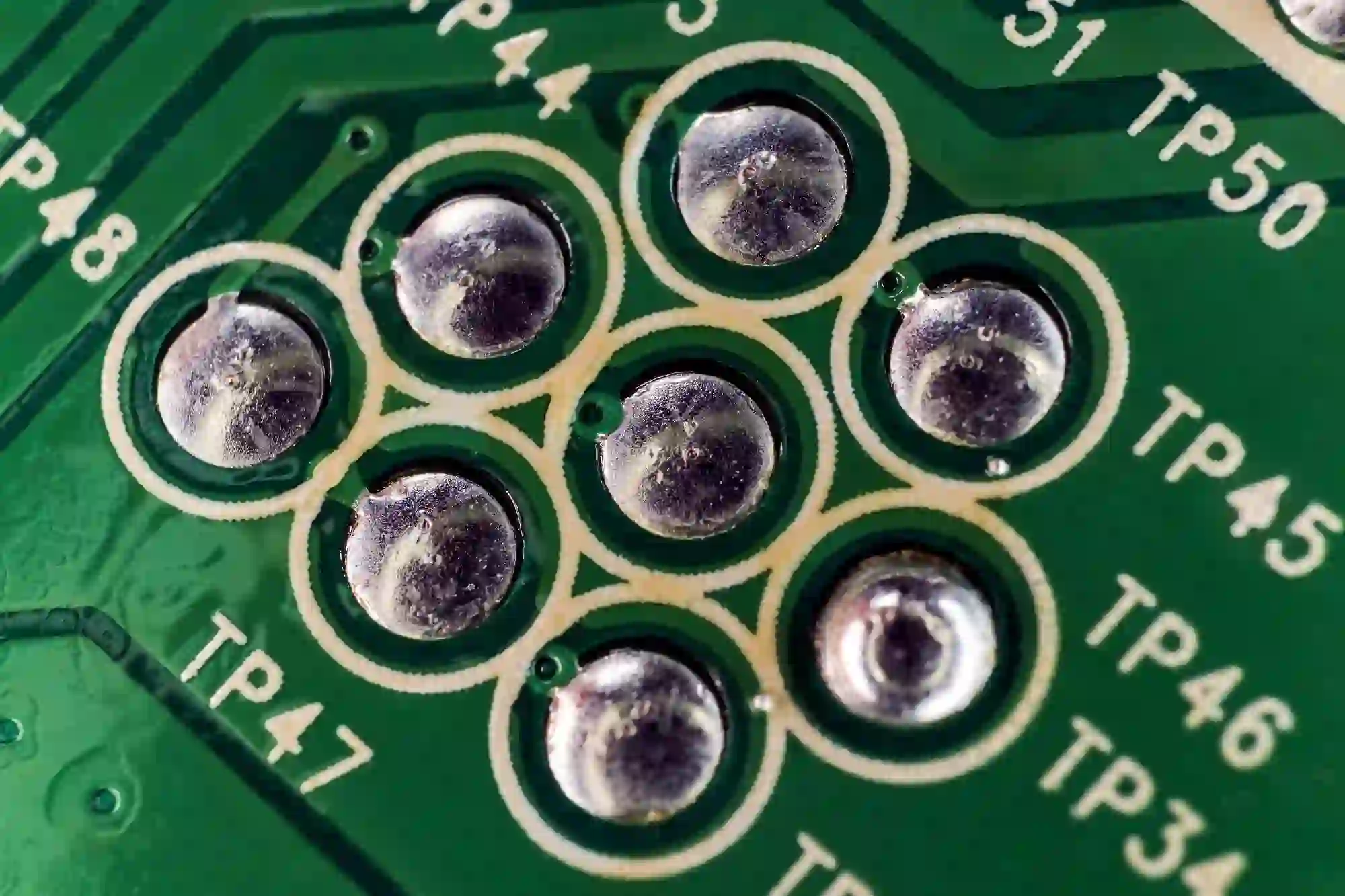
Solder joint reliability in space depends heavily on design. Avoid overly small or large joints—small joints lack mechanical strength, while large ones can create stress points due to uneven cooling. Aim for a concave fillet shape, which indicates proper wetting and bonding between the solder, pad, and component lead. A fillet height of 1.5 to 2 times the lead thickness is often ideal for through-hole components, as it balances strength and flexibility.
For surface-mount components, ensure pad sizes match manufacturer recommendations to prevent tombstoning (where one end of the component lifts during soldering). Use thermal relief patterns for ground planes to avoid heat dissipation issues during soldering, which can lead to cold joints.
3. Control Soldering Temperature and Time
Excessive heat during soldering can damage components or cause thermal shock to the PCB substrate, especially in materials like FR-4 or polyimide used in space applications. Use a soldering iron or reflow oven with precise temperature control, maintaining profiles within 20°C of the recommended peak for the solder alloy. For Sn63Pb37, this typically means a peak reflow temperature of 205-215°C for no more than 60-90 seconds.
Preheating the board to around 100-120°C before soldering minimizes thermal gradients, reducing the risk of cracking. For hand soldering, use a tip temperature of 300-350°C, applying heat for no longer than 3-5 seconds per joint to avoid overheating delicate components.
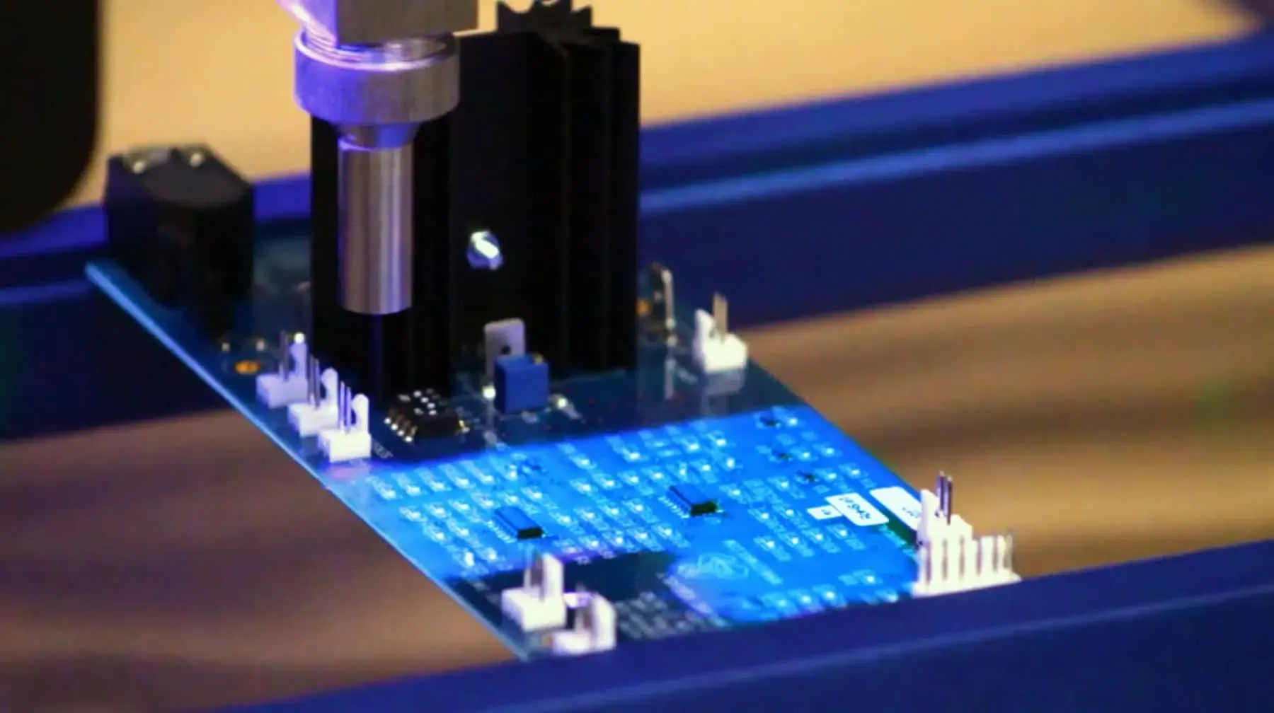
4. Implement Rigorous Inspection and Testing
Inspection is non-negotiable for space probe PCB assembly. Use automated optical inspection (AOI) systems to check for defects like insufficient solder, bridging, or misalignment. X-ray inspection is also valuable for hidden joints, such as those under ball grid array (BGA) components, ensuring no voids or cracks are present. Voids in solder joints can reduce thermal conductivity and mechanical strength, increasing failure risks under vibration or thermal cycling.
Post-assembly, subject PCBs to environmental testing, including thermal cycling between -55°C and +125°C for at least 100 cycles, as per standards like MIL-STD-883. Vibration testing at frequencies of 20-2000 Hz with amplitudes mimicking launch conditions ensures solder joints hold under stress.
PCB Assembly for Extreme Environments: Additional Considerations
1. Material Selection for PCBs
Beyond soldering, the choice of PCB materials impacts reliability in extreme environments. Standard FR-4 may suffice for some applications, but for space probes, high-performance materials like polyimide or ceramic substrates are better suited. Polyimide offers a glass transition temperature (Tg) above 200°C, ensuring stability under thermal stress, while ceramics provide excellent radiation resistance and thermal conductivity (often 20-30 W/m·K compared to FR-4’s 0.3 W/m·K).
Ensure that all materials are rated for low outgassing per ASTM E595, as volatile compounds released in a vacuum can degrade nearby optics or sensors.
2. Component Derating and Redundancy
In space, components must operate well below their maximum ratings to account for radiation and thermal stress. Derate components to 50-60% of their maximum voltage, current, or power specifications to extend lifespan. For critical systems, incorporate redundancy by duplicating key circuits, ensuring that a single point of failure doesn’t doom the mission.
The Role of Conformal Coating for Space Probe PCBs
Conformal coating is a protective layer applied to PCBs to shield them from environmental hazards. For space probe PCBs, conformal coating is essential to protect against moisture (during ground testing), radiation-induced corrosion, and mechanical stress. Common materials include silicone, acrylic, and parylene, each with unique benefits.
- Silicone: Offers excellent thermal stability, withstanding temperatures from -65°C to +200°C, making it ideal for thermal cycling in space.
- Acrylic: Provides good moisture resistance and is easier to apply or rework, though less durable under extreme temperatures.
- Parylene: A thin, uniform coating with superior dielectric properties (dielectric strength of 5,600 V/mil for a 1-mil layer) and low outgassing, perfect for vacuum environments.
Apply coatings evenly, with thicknesses typically between 25-75 micrometers, to avoid stress on solder joints. Ensure complete coverage around components, especially underfill areas, to prevent voids where contaminants could accumulate. Test coatings for adhesion and thermal performance per standards like IPC-CC-830 before deployment.
Ensuring Long-Term Solder Joint Reliability in Space
Solder joint reliability in space isn’t just about the initial assembly—it’s about sustained performance over years or decades. Fatigue from thermal cycling is a primary concern, as repeated expansion and contraction can cause microcracks. To mitigate this, use flexible solder alloys and design joints with slight compliance to absorb stress. Regularly simulate mission conditions during testing, monitoring for changes in joint resistance (ideally below 10 milliohms per joint) to predict potential failures.
Another factor is radiation hardening. High-energy particles can cause lattice defects in solder materials, weakening bonds over time. While no solder is immune to radiation, using gold-plated leads or radiation-resistant alloys can slow degradation. Pair this with strategic shielding of critical PCB areas to minimize exposure.
Partnering with Experts for Space Probe PCB Assembly
Assembling PCBs for space probes is a complex endeavor requiring specialized skills, equipment, and adherence to strict standards. At ALLPCB, we provide end-to-end solutions for high-reliability PCB assembly, from material selection to soldering and conformal coating. Our processes align with industry standards like NASA and MIL specifications, ensuring your assemblies are ready for the harshest environments. Whether you’re working on a small satellite or a deep-space explorer, our team is equipped to deliver precision and durability.
Conclusion
High-reliability soldering is the backbone of successful space probe missions. By mastering space probe PCB soldering techniques, optimizing solder joint reliability in space, and leveraging protective measures like conformal coating for space probe PCBs, engineers can build electronics that endure the rigors of space. From selecting the right materials to rigorous testing and design optimization, every step counts in PCB assembly for extreme environments. With these best practices, you can ensure your space-bound projects achieve mission success, no matter the challenges of the cosmos.


