 ALLPCB


In today’s world, smart water treatment is becoming a critical solution for managing water resources efficiently. At the heart of this transformation are advanced Printed Circuit Boards (PCBs) that power control systems for water management. These PCBs enable technologies like IoT water treatment control, remote monitoring, and intelligent water grids, ensuring cleaner, safer, and more sustainable water systems. In this blog, we’ll explore how cutting-edge PCB designs are driving innovation in smart water management and automated water treatment plants, delivering precise control and real-time data for better decision-making.
The Growing Need for Smart Water Treatment Solutions
Water scarcity, pollution, and aging infrastructure are pressing challenges globally. With urban populations growing and industrial demands rising, traditional water treatment methods are often inefficient and costly. Smart water treatment systems, powered by advanced technologies, offer a way to optimize resources, reduce waste, and ensure compliance with strict environmental standards.
At the core of these systems are control units that rely on high-performance PCBs. A smart water management PCB integrates sensors, microcontrollers, and communication modules to monitor water quality, control treatment processes, and transmit data in real time. These PCBs are designed to withstand harsh environments, ensuring reliability in water treatment plants where humidity and temperature fluctuations are common.
How PCBs Power IoT Water Treatment Control
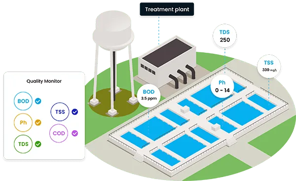
The Internet of Things (IoT) has transformed water treatment by enabling real-time monitoring and automation. IoT water treatment control systems use sensors to measure parameters like pH levels, turbidity, and chemical concentrations, sending this data to centralized systems for analysis. PCBs play a vital role by acting as the backbone of these IoT devices, ensuring seamless connectivity and data accuracy.
For instance, a typical IoT-enabled PCB for water treatment might include a low-power microcontroller operating at 3.3V, paired with a Wi-Fi or LoRa module for long-range communication. These boards often feature analog-to-digital converters (ADCs) with a resolution of 12 bits or higher to process sensor data with precision. Such specifications allow the system to detect even minor changes in water quality, triggering automated responses like adjusting chemical dosing pumps within milliseconds.
By integrating IoT with custom-designed PCBs, water treatment plants can reduce manual intervention, lower operational costs, and improve response times to potential issues. This technology ensures that water quality remains consistent, even in remote or unmanned facilities.
PCB Remote Monitoring Systems: Real-Time Insights for Water Management
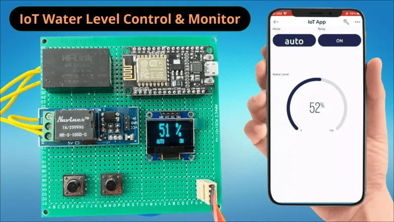
One of the standout benefits of modern water treatment technology is remote monitoring. PCB remote monitoring systems allow operators to track water quality and system performance from anywhere in the world. These systems rely on robust PCB designs that support wireless communication protocols such as 4G, 5G, or satellite connections, ensuring uninterrupted data flow even in isolated locations.
A well-designed PCB for remote monitoring might include a power management circuit to optimize energy use, often operating at an efficiency of over 90%. This is critical for battery-powered devices in remote areas where power supply is limited. Additionally, these PCBs are often built with impedance-controlled traces to maintain signal integrity over long distances, ensuring that data transmission remains reliable with minimal latency—often under 100 milliseconds for critical alerts.
With PCB remote monitoring systems, water treatment facilities can detect leaks, equipment failures, or contamination events instantly, preventing costly downtime and environmental damage. This capability is especially valuable for municipalities managing large-scale water grids across multiple locations.
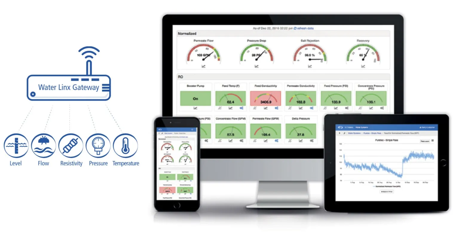
Intelligent Water Grids: The Role of Specialized PCBs
Intelligent water grids represent the future of water distribution and treatment. These grids use a network of sensors, actuators, and control systems to manage water flow, pressure, and quality across vast areas. An intelligent water grids PCB is designed to handle complex tasks, such as coordinating data from thousands of endpoints while ensuring low power consumption and high reliability.
For example, PCBs in intelligent water grids often incorporate multi-layer designs—sometimes with 8 or more layers—to accommodate the high density of components needed for processing and communication. These boards may use high-speed signal paths with controlled impedance of 50 ohms to prevent data loss during transmission. They also feature robust shielding to protect against electromagnetic interference (EMI), which is common in industrial environments.
By leveraging these specialized PCBs, intelligent water grids can balance supply and demand, detect pipe leaks with precision (often within a margin of 1 meter), and optimize energy use for pumping systems. This results in significant cost savings and a reduced environmental footprint for water utilities.
PCBs for Automated Water Treatment Plants: Precision and Efficiency
Automation is a game-changer for water treatment plants, allowing for 24/7 operation with minimal human oversight. A PCB for automated water treatment plants is engineered to control multiple processes simultaneously, from filtration and chemical dosing to backwashing and sludge removal. These PCBs are often customized to handle high current loads—sometimes up to 10A or more—for driving motors and pumps, while also supporting low-voltage circuits for sensor integration.
A key feature of these PCBs is their ability to operate in harsh conditions. They are typically coated with conformal coatings to protect against moisture and corrosion, ensuring a lifespan of 10 years or more even in humid environments. Additionally, they often include built-in fault detection circuits that monitor voltage drops or current spikes, alerting operators to potential issues before they escalate.
Automated water treatment plants equipped with such PCBs can achieve up to 30% higher efficiency in water processing compared to manual systems. They also reduce chemical overuse by precisely controlling dosages based on real-time sensor feedback, which can lower operational costs by 15-20% annually.
Key Design Considerations for Smart Water Treatment PCBs
Designing a PCB for smart water treatment applications requires careful planning to meet the unique demands of the industry. Here are some critical factors that engineers prioritize:
- Durability: PCBs must resist moisture, chemicals, and temperature extremes. Materials like FR-4 with high glass transition temperatures (Tg of 170°C or above) are often used for their thermal stability.
- Power Efficiency: Many devices in remote or IoT setups rely on battery power. PCBs are designed with low-power components and sleep modes to extend battery life, often achieving standby currents as low as 10 microamps.
- Signal Integrity: High-speed data transmission is essential for real-time monitoring. PCBs are engineered with controlled impedance traces and minimal crosstalk, ensuring signal speeds of up to 1 Gbps for critical applications.
- Scalability: As water treatment systems expand, PCBs must support modular designs that allow for easy upgrades or integration with new sensors and communication protocols.
- Compliance: PCBs must meet industry standards like IPC-A-610 for manufacturing quality and RoHS for environmental safety, ensuring they are safe for use in water-related applications.
By addressing these design challenges, manufacturers can produce PCBs that deliver long-term reliability and performance in smart water treatment systems.
Benefits of Advanced PCBs in Smart Water Treatment
The integration of advanced PCBs into water treatment systems offers numerous advantages for both operators and end-users. Here are some of the most impactful benefits:
- Enhanced Accuracy: PCBs with high-resolution ADCs and precise control circuits ensure accurate monitoring and adjustment of water treatment processes, maintaining water quality within regulatory limits.
- Cost Savings: Automation and remote monitoring reduce labor costs and prevent expensive repairs by detecting issues early. Some facilities report savings of up to 25% on maintenance expenses.
- Sustainability: Optimized processes driven by smart PCBs minimize water and energy waste, supporting environmental goals. For instance, intelligent grids can reduce water loss from leaks by up to 40%.
- Scalable Solutions: Modular PCB designs allow water treatment systems to grow with demand, whether for a small rural plant or a sprawling urban grid.
- Improved Safety: Real-time alerts and automated responses prevent contamination events, protecting public health and avoiding costly fines for non-compliance.
These benefits highlight why investing in high-quality PCB designs is essential for modern water treatment infrastructure.
Future Trends: What’s Next for PCBs in Water Treatment?
The role of PCBs in smart water treatment is set to expand as technology advances. Emerging trends include the integration of artificial intelligence (AI) directly onto PCBs, enabling predictive maintenance and adaptive control without relying on external servers. This could reduce latency in decision-making to under 50 milliseconds, a critical improvement for large-scale systems.
Additionally, the adoption of 5G technology will enhance PCB remote monitoring systems, offering data transfer rates of up to 10 Gbps for ultra-fast communication across intelligent water grids. Miniaturization is another focus, with PCBs becoming smaller yet more powerful thanks to advancements in surface-mount technology (SMT) and high-density interconnects (HDI), allowing for compact designs in space-constrained setups.
As water challenges grow, the demand for innovative PCB solutions will only increase, driving further research into materials, connectivity, and energy efficiency. Staying ahead of these trends ensures that water treatment facilities remain resilient and future-ready.
Conclusion: Building Smarter Water Systems with Advanced PCBs
Advanced PCBs are at the forefront of revolutionizing smart water treatment, powering everything from IoT water treatment control to intelligent water grids. By enabling precise monitoring, automation, and real-time data analysis, these PCBs help address global water challenges with efficiency and sustainability. Whether it’s a smart water management PCB for a small facility or a complex design for an automated water treatment plant, the right technology can make all the difference.
At ALLPCB, we’re committed to supporting the water treatment industry with high-quality, custom PCB solutions tailored to the unique demands of this field. By partnering with us, engineers and facility managers can access the tools needed to build smarter, more reliable water systems for a better tomorrow.


