ALLPCB


In the fast-evolving world of defense electronics, creating smaller, lighter, and more efficient systems is critical. High-Density Interconnect (HDI) PCBs play a vital role in achieving this goal, especially for compact missile systems. These advanced circuit boards allow for tighter component packing and improved performance in limited spaces, making them ideal for missile guidance and other defense applications. If you're exploring HDI PCB design for missile guidance, microvia PCB technology, or miniaturization in defense electronics, this blog will guide you through the essentials of HDI PCBs and their impact on modern missile systems.
In this comprehensive guide, we'll dive into the importance of miniaturization, the unique features of HDI PCBs, and how they address the challenges of designing for compact missile systems. From blind and buried vias for missile PCBs to high-density component placement, we'll cover the key aspects that make HDI technology a game-changer in the defense sector. Let’s explore how these tiny yet powerful boards are shaping the future of military innovation.
Why Miniaturization is Critical in Missile Systems
Missile systems demand cutting-edge technology to meet strict size, weight, and performance requirements. As modern warfare shifts toward precision and agility, the need for compact electronics has never been greater. Miniaturization allows for smaller, lighter missile designs that can be deployed more efficiently, whether launched from aircraft, ships, or ground platforms. Reducing the size of electronic components also means more room for other critical systems, like propulsion or payload.
In missile guidance systems, every gram and cubic centimeter counts. Smaller PCBs mean reduced weight, which can improve the missile's range and speed. Additionally, compact designs often lead to lower power consumption, a crucial factor for systems that must operate reliably over long missions. HDI PCBs are at the heart of this transformation, enabling engineers to pack more functionality into less space without sacrificing performance.

What Are HDI PCBs and Why Do They Matter?
High-Density Interconnect (HDI) PCBs are a type of printed circuit board designed to maximize wiring density in a smaller footprint. Unlike traditional PCBs, HDI boards use advanced manufacturing techniques to create finer lines, smaller vias, and tighter spacing between components. This results in a board that can handle more complex circuits while taking up less space—a perfect fit for the demands of missile systems.
HDI PCBs stand out due to their ability to support high-speed signals with minimal interference. In missile guidance systems, where data must be processed in real-time to ensure accuracy, maintaining signal integrity is non-negotiable. HDI technology achieves this by reducing the distance signals travel and minimizing crosstalk between traces. For example, HDI boards often support signal speeds exceeding 10 Gbps, critical for rapid communication in defense applications.
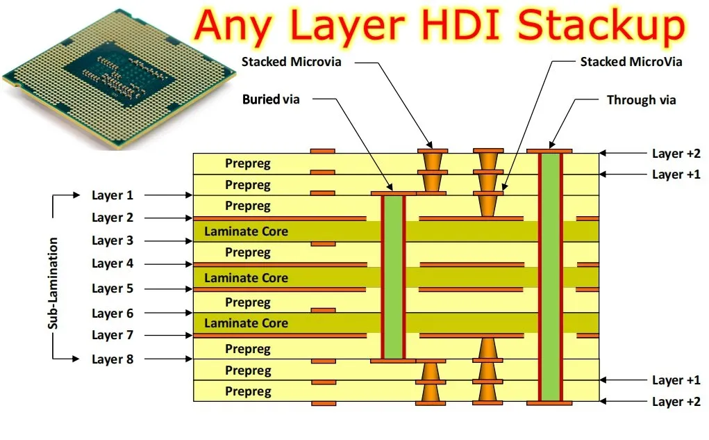
Moreover, HDI PCBs often incorporate multiple layers—sometimes 8 or more—in a much thinner profile than conventional boards. This multilayer approach allows for greater functionality without increasing the board's size, directly supporting miniaturization in defense electronics.
Key Features of HDI PCBs for Missile Systems
HDI PCBs are packed with features that make them indispensable for compact missile systems. Below, we break down the most important aspects and explain how they contribute to performance and reliability in defense applications.
1. Microvia PCB Technology
One of the defining characteristics of HDI PCBs is the use of microvias—tiny holes drilled with lasers to connect different layers of the board. Unlike traditional through-hole vias, which pass through the entire board and take up valuable space, microvias are much smaller, often less than 0.15 mm in diameter. This allows for denser routing and more efficient use of board space, a must-have for missile guidance systems.
Microvia PCB technology also improves electrical performance. Because microvias are shorter, they reduce signal loss and inductance, ensuring faster and more reliable data transmission. In a missile system, where split-second decisions can determine success or failure, this enhanced performance is invaluable.
2. Blind and Buried Vias for Missile PCBs
Another key feature of HDI PCBs is the use of blind and buried vias for missile PCBs. Blind vias connect an outer layer of the board to an inner layer without passing through the entire board, while buried vias connect only internal layers and are not visible on the surface. Both types save space on the outer layers, allowing for more components or routing in a smaller area.
In missile systems, where every millimeter of PCB space is critical, blind and buried vias enable designers to create highly compact layouts. They also reduce the risk of signal interference by keeping connections shorter and more direct. For instance, a typical HDI board for defense applications might use blind vias with an aspect ratio of 1:1, ensuring reliable connections without compromising on space.
3. High-Density Component Placement
High-density component placement is at the core of HDI PCB design. By using finer traces (often less than 0.1 mm wide) and smaller pads, HDI boards can accommodate more components in a smaller area. This is particularly important for missile guidance systems, which often require multiple sensors, processors, and communication modules on a single board.
For example, an HDI PCB might support component densities of over 150 components per square inch, compared to just 50 on a traditional board. This level of density allows engineers to integrate complex functionalities—such as real-time data processing and navigation—into a board small enough to fit inside a missile's limited space.
4. Multilayer Design for Enhanced Functionality
HDI PCBs often feature multiple layers stacked together, sometimes exceeding 12 layers in advanced designs. This multilayer structure allows for separate power, ground, and signal planes, reducing noise and improving overall performance. In missile systems, where electromagnetic interference (EMI) can disrupt critical operations, this design is essential for maintaining reliability.
Additionally, multilayer HDI boards can handle higher current densities, often up to 20 A per square inch, ensuring they can power demanding components without overheating. This makes them ideal for the harsh operating conditions of defense applications.
Benefits of HDI PCBs in Missile Guidance Systems
The adoption of HDI PCBs in HDI PCB design for missile guidance brings several advantages that directly impact the performance and reliability of missile systems. Let’s explore some of the most significant benefits.
1. Space and Weight Savings
As mentioned earlier, HDI PCBs are much smaller and lighter than traditional boards. A typical HDI board might be 30% thinner and 25% lighter than a conventional PCB with similar functionality. In missile systems, this translates to reduced overall weight, allowing for longer ranges or higher payloads.
2. Improved Signal Integrity
Signal integrity is paramount in missile guidance systems, where even a small delay or error can lead to mission failure. HDI PCBs minimize signal loss by using shorter traces and microvias, often achieving impedance values as precise as 50 ohms for high-speed signals. This ensures accurate data transmission, even in high-stress environments.
3. Enhanced Reliability Under Harsh Conditions
Missile systems operate in extreme conditions, from high temperatures to intense vibrations. HDI PCBs are built to withstand these challenges, often using advanced materials with thermal coefficients of expansion (CTE) as low as 15 ppm/°C. This ensures the board remains stable and functional, no matter the environment.
4. Cost Efficiency in the Long Run
While HDI PCBs may have a higher upfront cost due to their complex manufacturing process, they often save money over time. By reducing the number of boards needed in a system and improving reliability, they lower maintenance and replacement costs. For defense projects with tight budgets, this long-term efficiency is a major advantage.

Challenges in Designing HDI PCBs for Defense Applications
While HDI PCBs offer numerous benefits, designing them for missile systems is not without challenges. Engineers must navigate several hurdles to ensure the boards meet the strict requirements of defense applications.
1. Complex Manufacturing Processes
Creating HDI PCBs involves advanced techniques like laser drilling for microvias and sequential lamination for multilayer designs. These processes require precision and expertise, as even a small error can lead to signal issues or board failure. For missile systems, where reliability is critical, manufacturers must adhere to strict quality standards.
2. Thermal Management
High-density designs generate more heat in a smaller area, which can be problematic in missile systems with limited cooling options. Engineers must carefully select materials with high thermal conductivity—often exceeding 1.5 W/mK—and design layouts that dissipate heat effectively.
3. Compliance with Military Standards
Defense electronics must comply with rigorous standards for durability, EMI shielding, and performance. HDI PCBs for missile systems often need to meet specifications like MIL-PRF-31032, ensuring they can withstand the unique stresses of military use.
How HDI PCBs Drive Innovation in Defense Electronics
Beyond missile systems, HDI PCBs are driving broader innovation in miniaturization in defense electronics. From drones to wearable soldier systems, the ability to pack more power into smaller devices is transforming how military technology is developed. HDI technology enables faster communication systems, more accurate sensors, and more efficient power management—all critical for modern defense operations.
For instance, HDI PCBs are increasingly used in satellite communication systems, where space and weight constraints are even more severe than in missiles. By leveraging the same principles of high-density design, engineers can create systems that push the boundaries of what’s possible in defense technology.
Best Practices for Designing HDI PCBs for Missile Systems
For engineers looking to implement HDI PCBs in missile guidance systems, following best practices is essential for success. Here are some actionable tips to keep in mind:
- Optimize Layer Stackup: Plan the layer stackup early in the design process to balance signal integrity and thermal performance. Use dedicated ground planes to minimize EMI.
- Use Advanced Simulation Tools: Leverage simulation software to test signal paths and thermal behavior before manufacturing. This can prevent costly redesigns.
- Select the Right Materials: Choose substrates with low dielectric constants (often below 3.5) to support high-speed signals and materials with high thermal resistance for durability.
- Focus on Via Placement: Strategically place microvias, blind, and buried vias to maximize routing density without compromising reliability.
- Partner with Experienced Manufacturers: Work with a trusted PCB provider who understands the unique demands of defense applications and can deliver high-quality HDI boards.

Conclusion: The Future of HDI PCBs in Missile Systems
As the defense industry continues to prioritize precision, efficiency, and compactness, HDI PCBs will remain a cornerstone of innovation. Their ability to support high-density component placement, leverage microvia PCB technology, and incorporate blind and buried vias for missile PCBs makes them indispensable for modern missile guidance systems. By enabling miniaturization in defense electronics, HDI technology is helping to create smarter, faster, and more reliable military solutions.
At ALLPCB, we’re committed to supporting engineers in pushing the boundaries of what’s possible with HDI PCB design. Whether you’re working on missile systems or other cutting-edge defense projects, our expertise and advanced manufacturing capabilities can help bring your vision to life. Explore the power of HDI technology and see how it can transform your next project.