 ALLPCB


Flexible PCBs are a game-changer in modern electronics, allowing designs to bend and fit into compact or dynamic spaces. However, one critical factor often overlooked is line width tolerance in flexible PCBs, especially when bending is involved. How does line width tolerance impact the performance and reliability of a flex PCB under bending stress? Simply put, maintaining precise line widths within tight tolerances is essential to prevent signal loss, cracking, or failure during bending. In this blog, we'll dive deep into the challenges of flexible PCB line width, flex PCB tolerance, bending radius, polyimide PCB materials, and flexible circuit design to help engineers navigate these complexities.
What is Line Width Tolerance in Flexible PCBs?
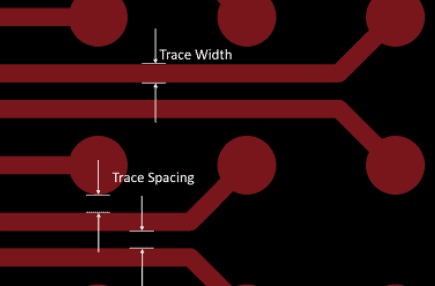
Line width tolerance refers to the acceptable variation in the width of conductive traces on a PCB. In flexible PCBs, these traces are often made of copper and are critical for carrying electrical signals. Unlike rigid PCBs, flex PCBs face additional stress from bending, twisting, and folding, making tolerance even more crucial. A typical line width tolerance for flexible PCBs might range from ±10% to ±20%, depending on the manufacturing process and design requirements. For instance, a trace designed to be 0.1 mm wide might actually vary between 0.08 mm and 0.12 mm if a ±20% tolerance is applied.
Why does this matter? Variations in line width can affect impedance, signal integrity, and current-carrying capacity. In high-frequency applications, even a small deviation can lead to signal degradation. When bending is added to the mix, inconsistent line widths may cause stress concentration, leading to cracks or breaks in the copper traces. Understanding and controlling flex PCB tolerance is, therefore, a foundational step in ensuring reliability.
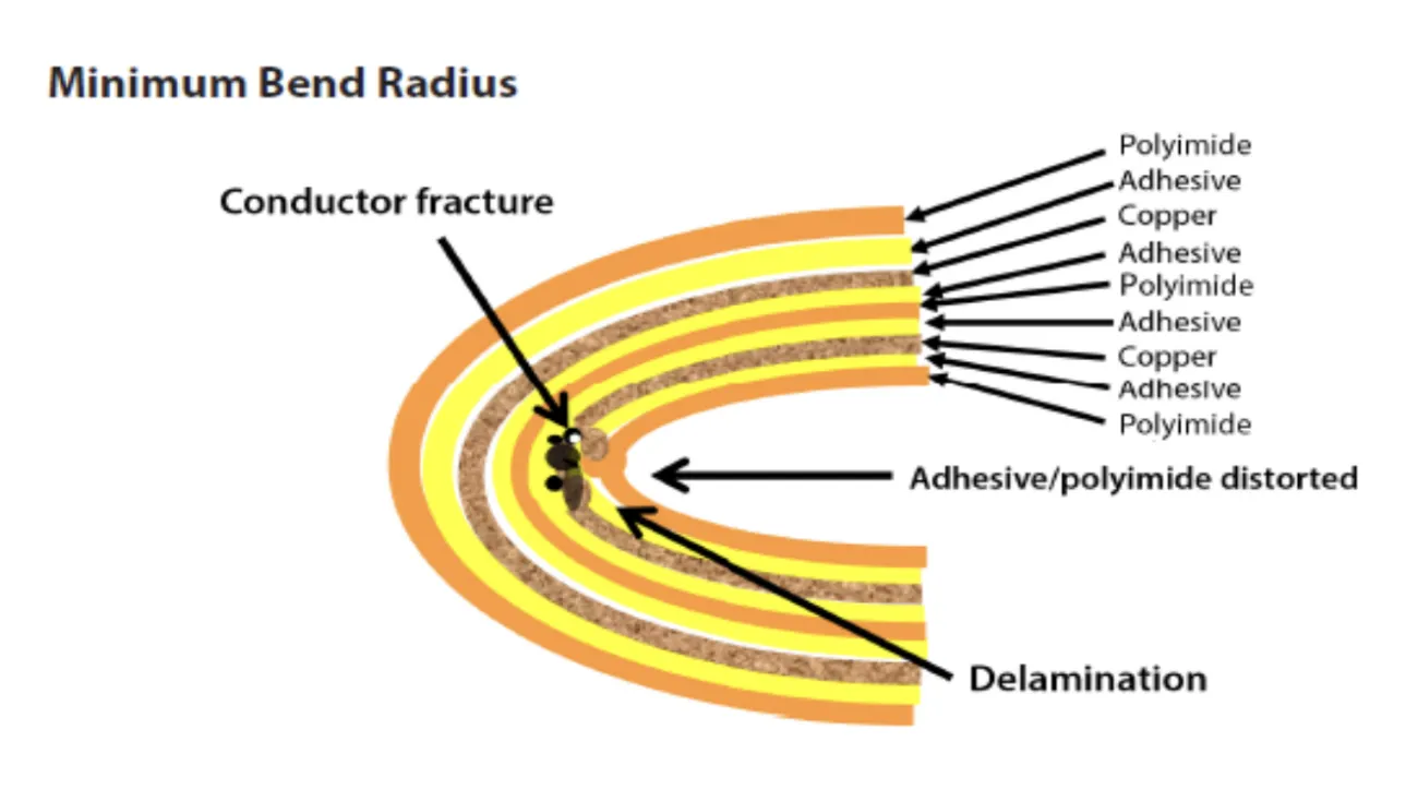
The Role of Bending Radius in Flexible PCB Design
The bending radius is the minimum radius a flexible PCB can be bent without damaging the board or its components. It directly impacts how much stress is applied to the copper traces and the substrate material, often polyimide, during flexing. A smaller bending radius means tighter bends and higher stress, which can exacerbate issues caused by poor line width tolerance.
Industry standards, such as those from the IPC (Institute of Printed Circuits), suggest that the bending radius should be at least 6 to 10 times the thickness of the flex PCB for dynamic applications (where bending occurs repeatedly). For a 0.2 mm thick flex PCB, this translates to a minimum bending radius of 1.2 to 2 mm. If the line width tolerance is not tightly controlled, areas with thinner traces may crack under this stress, while thicker traces might cause uneven impedance.
Designing with the correct bending radius is not just about avoiding physical damage. It also ensures that signal integrity is maintained, especially for high-speed signals where impedance matching is critical. For example, a 50-ohm impedance line on a flex PCB must maintain consistent width and spacing to avoid reflections or losses, even when bent.
Polyimide PCB: The Backbone of Flexible Circuits
Polyimide is the most common substrate material for flexible PCBs due to its excellent thermal stability, flexibility, and durability. It can withstand temperatures up to 400°C and offers a high tensile strength, making it ideal for applications where bending and environmental stress are factors. However, even polyimide has its limits when it comes to line width tolerance and bending challenges.
The thinness of polyimide layers, often between 0.025 mm and 0.125 mm, allows for tight bending radii. But this thinness also means that any variation in copper trace width can create weak points. During manufacturing, the etching process used to create traces on polyimide must be precisely controlled to achieve consistent line widths. A deviation of just 0.01 mm in a 0.1 mm trace can lead to a 10% change in impedance, which is significant for high-frequency designs operating at 1 GHz or above.
Additionally, polyimide's flexibility can lead to uneven stress distribution if the PCB design does not account for bending areas. Designers must ensure that traces in bending zones are either wider or reinforced to handle the mechanical stress, balancing this with the need for precise tolerances to maintain electrical performance.
Flexible Circuit Design Challenges with Line Width Tolerance
Designing a flexible PCB is inherently more complex than designing a rigid one, and line width tolerance adds another layer of difficulty. Here are some of the key challenges engineers face:
1. Balancing Electrical and Mechanical Requirements
Flexible circuit design requires a delicate balance between electrical performance and mechanical durability. Narrow traces are often needed for high-density designs or to achieve specific impedance values, such as 50 ohms for RF signals. However, narrower traces are more prone to breaking under bending stress if the tolerance is not tightly controlled. A trace designed at 0.075 mm might end up at 0.06 mm due to manufacturing variations, significantly increasing the risk of failure.
To mitigate this, designers can use wider traces in bending areas, but this might not always be feasible due to space constraints or electrical requirements. Another option is to route critical traces away from high-stress bending zones, though this can complicate the layout.
2. Manufacturing Limitations
Manufacturing flexible PCBs with tight line width tolerances is challenging due to the nature of the materials and processes involved. The etching process, for instance, can result in under-etching or over-etching, leading to traces that are too wide or too narrow. For a flex PCB with a target line width of 0.1 mm, achieving a tolerance of ±10% (0.09 mm to 0.11 mm) requires advanced equipment and skilled operators. Many manufacturers struggle to maintain tolerances below ±15%, especially for high-volume production.
This limitation means designers must often work within broader tolerance ranges, which can impact performance. Collaborating closely with the fabrication team during the design phase can help set realistic expectations and optimize the design for manufacturability.
3. Signal Integrity Under Bending Stress
Signal integrity is a major concern in flexible PCBs, especially for high-speed or high-frequency applications. Variations in line width due to tolerance issues can cause impedance mismatches, leading to signal reflections and losses. For a differential pair designed to operate at 5 Gbps, a line width variation of just 0.02 mm can shift the impedance from the target 100 ohms to 110 ohms, introducing unwanted noise and reducing signal quality.
Bending exacerbates this issue by altering the spacing between traces and the dielectric properties of the substrate. Designers must simulate bending conditions during the design phase to predict how line width variations will affect performance and adjust accordingly.
Best Practices for Managing Line Width Tolerance in Flex PCB Design
To overcome the challenges of line width tolerance and bending in flexible PCBs, engineers can follow these best practices:
1. Define Realistic Tolerances Early
Work with your manufacturing partner to understand their capabilities and define achievable line width tolerances. If a tolerance of ±10% is not feasible, adjust your design to accommodate a broader range, such as ±15%, while still meeting performance goals. For critical traces, consider specifying tighter tolerances only where necessary to keep costs manageable.
2. Use Design Software for Simulation
Modern PCB design tools allow you to simulate bending and stress conditions, helping identify potential weak points caused by line width variations. These simulations can also predict impedance changes and signal integrity issues, enabling you to refine your design before fabrication. Aim for a design that maintains consistent performance even under worst-case tolerance scenarios.
3. Reinforce Bending Areas
In areas prone to frequent bending, consider reinforcing traces by increasing their width or adding stiffeners to the PCB. Stiffeners, often made of additional polyimide or FR4 material, can reduce stress on critical traces, improving reliability without sacrificing flexibility in other areas.
4. Optimize Trace Routing
Route high-speed or critical traces away from bending zones whenever possible. If traces must pass through these areas, orient them perpendicular to the bend to minimize stress. Additionally, avoid sharp corners in trace routing, as they can act as stress concentrators and increase the risk of cracking, especially if line width tolerance is not tightly controlled.
5. Test Prototypes Under Real Conditions
Before moving to full-scale production, test your flexible PCB prototypes under real-world bending and environmental conditions. Measure signal integrity, impedance, and mechanical durability to ensure that line width tolerances do not compromise performance. Use these results to make any necessary design adjustments.
Conclusion: Mastering Flexible PCB Design with Tolerance in Mind
Line width tolerance in flexible PCBs is a critical factor that can make or break the reliability and performance of your design, especially when bending is involved. By understanding the interplay between flex PCB tolerance, bending radius, and polyimide PCB materials, engineers can create robust flexible circuit designs that withstand mechanical stress while maintaining electrical integrity. From defining realistic tolerances to simulating bending conditions and reinforcing critical areas, the strategies outlined in this blog provide a roadmap for success.
Whether you're working on a wearable device, automotive sensor, or medical implant, paying close attention to flexible PCB line width and tolerance will help you avoid costly failures and ensure long-term reliability. With careful planning and collaboration with your manufacturing partner, you can tackle the bending challenge head-on and bring your innovative designs to life.


