 ALLPCB


In the fast-evolving world of healthcare technology, IoT-enabled patient monitoring systems are transforming how medical professionals track and manage patient health. At the heart of these systems are printed circuit boards (PCBs) designed specifically for IoT applications in medical devices. However, creating effective IoT PCB design for medical devices comes with significant challenges, particularly in connectivity and security. This blog dives deep into these challenges and explores how innovative PCB solutions address issues like wireless PCB security, data encryption for patient monitoring, low-power IoT PCB designs, secure data transmission PCB techniques, and the role of 5G PCB medical applications.
Whether you're an engineer designing the next generation of wearable health trackers or a healthcare innovator looking to integrate IoT solutions, this guide will provide actionable insights to help you navigate the complexities of IoT-enabled patient monitoring PCBs.
The Rise of IoT in Patient Monitoring Systems
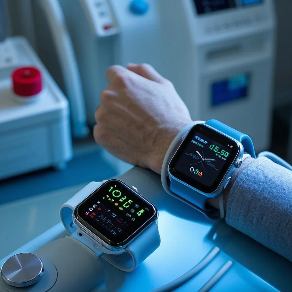
The Internet of Things (IoT) has revolutionized healthcare by enabling real-time patient monitoring through connected devices. Wearable sensors, remote health trackers, and implantable devices now collect vital data such as heart rate, blood pressure, and oxygen levels, transmitting this information to healthcare providers instantly. PCBs are the backbone of these devices, ensuring seamless connectivity and reliable performance.
However, with this connectivity comes the dual challenge of maintaining robust communication and protecting sensitive patient data. As IoT devices become more integrated into medical applications, the demand for specialized PCB designs that prioritize both connectivity and security continues to grow.
Key Challenges in IoT PCB Design for Medical Devices
Designing PCBs for IoT-enabled patient monitoring systems is no easy task. Engineers must address several critical challenges to ensure the devices are safe, reliable, and effective. Below, we break down the most pressing issues and how they can be tackled.
1. Connectivity Challenges in Wireless PCB Design
IoT medical devices rely heavily on wireless communication to transmit data to healthcare systems. This requires PCBs to support protocols like Bluetooth, Wi-Fi, and increasingly, 5G for faster and more reliable connections. However, maintaining stable connectivity in environments with interference, such as hospitals with numerous electronic devices, is a significant hurdle.
For instance, a PCB designed for a wearable heart monitor must handle signal integrity at frequencies up to 2.4 GHz for Bluetooth or higher for 5G applications. Poor antenna placement or inadequate grounding can lead to signal loss or delays, which could be life-threatening in critical care scenarios. To overcome this, engineers often use high-frequency laminates with dielectric constants around 3.0 to 4.0 to minimize signal loss and ensure reliable performance.
Additionally, 5G PCB medical applications are gaining traction due to their ultra-low latency (as low as 1 millisecond) and high bandwidth, enabling real-time data streaming for remote surgeries or continuous monitoring. Designing PCBs for 5G requires precise impedance matching (typically 50 ohms) and advanced multilayer structures to handle high-speed signals without interference.
2. Security Concerns with Wireless PCB Data Transmission
One of the most critical issues in IoT patient monitoring is ensuring wireless PCB security. Medical devices transmit highly sensitive data, and any breach could compromise patient privacy or even lead to malicious interference with device functionality. Cybersecurity threats like hacking and data interception are real risks in wireless systems.
To address this, secure data transmission PCB designs incorporate hardware-based security features. For example, integrating secure microcontrollers with built-in encryption modules ensures that data is protected at the source. Advanced Encryption Standard (AES) with 256-bit keys is commonly used to encrypt data before transmission, making it nearly impossible for unauthorized parties to access.
Moreover, engineers can design PCBs with dedicated security layers, such as tamper-detection circuits that trigger alerts if physical interference is detected. These measures are essential for protecting patient data and maintaining trust in IoT medical devices.
3. Data Encryption for Patient Monitoring Systems
Closely tied to security is the need for robust data encryption in patient monitoring. Encryption ensures that data remains unreadable to unauthorized users during transmission from the device to the cloud or healthcare provider's servers. Without encryption, intercepted data could reveal sensitive health information, violating privacy regulations like HIPAA (Health Insurance Portability and Accountability Act).
In practice, encryption protocols are embedded into the firmware of IoT devices, but the PCB must support the necessary processing power to handle encryption without slowing down data transmission. For instance, a typical IoT medical device might process data at a rate of 1 Mbps, and encryption algorithms must operate within this constraint to avoid delays. Using low-power cryptographic hardware accelerators on the PCB can achieve this balance, ensuring both security and performance.
4. Power Efficiency with Low-Power IoT PCB Designs
Many IoT medical devices, such as wearable monitors, rely on battery power, making energy efficiency a top priority. A low-power IoT PCB design is crucial for extending battery life, especially for devices that need to operate continuously for days or weeks.
Engineers achieve low power consumption by using components with minimal quiescent current (often in the range of microamperes) and implementing sleep modes that reduce power usage when the device is idle. For example, a PCB for a blood glucose monitor might consume less than 10 mW in active mode and drop to under 1 μW in sleep mode. Additionally, selecting energy-efficient communication protocols like Bluetooth Low Energy (BLE) can further reduce power demands, with typical current draws of around 10 mA during transmission.
Multilayer PCB designs also help by optimizing trace layouts to minimize parasitic capacitance, which can otherwise lead to unnecessary power loss. These strategies ensure that IoT medical devices remain operational for longer periods, improving patient convenience and reducing maintenance needs.
Innovative Solutions for IoT PCB Design in Medical Devices
With the challenges outlined, let’s explore the cutting-edge solutions that are shaping the future of IoT-enabled patient monitoring PCBs. These advancements not only address connectivity and security issues but also pave the way for more reliable and efficient medical devices.
1. Advanced Materials for High-Performance PCBs
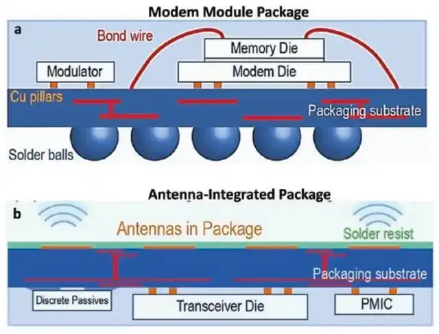
The choice of materials in PCB design plays a critical role in overcoming connectivity challenges. For high-frequency applications like 5G PCB medical applications, materials with low dielectric loss (such as PTFE-based laminates with a loss tangent of 0.002 or lower) are used to maintain signal integrity. These materials support faster data rates and reduce the risk of signal degradation over long distances.
Additionally, flexible and rigid-flex PCBs are increasingly popular for wearable medical devices. These boards can conform to the shape of the device, reducing size and weight while maintaining durability. For instance, a flexible PCB in a smart wristband can withstand bending cycles of over 100,000 without failure, ensuring long-term reliability.
2. Integration of IoT and Security Protocols
To enhance wireless PCB security, modern IoT PCBs are designed with integrated security protocols from the ground up. Secure boot mechanisms ensure that only authorized firmware runs on the device, preventing malicious code from taking control. Hardware security modules (HSMs) on the PCB can store encryption keys securely, reducing the risk of key theft even if the device is physically accessed.
Furthermore, over-the-air (OTA) update capabilities allow manufacturers to patch security vulnerabilities remotely, ensuring that devices remain protected against evolving threats. These features are vital for maintaining the integrity of patient monitoring systems in an increasingly connected world.
3. Leveraging 5G for Real-Time Monitoring
The rollout of 5G technology is a game-changer for IoT in healthcare. With download speeds up to 10 Gbps and latency as low as 1 ms, 5G enables real-time data transmission for applications like remote surgery and high-definition video consultations. PCBs designed for 5G PCB medical applications must support millimeter-wave frequencies (24-40 GHz), requiring precise design techniques such as microstrip transmission lines and advanced shielding to prevent crosstalk.
The result is a new generation of IoT medical devices capable of transmitting large volumes of data instantly, improving the speed and accuracy of patient care.
Best Practices for Designing Secure and Connected IoT PCBs
For engineers and designers working on IoT patient monitoring systems, following best practices can make a significant difference in overcoming connectivity and security challenges. Here are some actionable tips to keep in mind:
- Optimize Antenna Design: Place antennas away from noisy components and use simulation tools to ensure impedance matching (typically 50 ohms) for maximum signal strength.
- Prioritize Security Features: Integrate hardware encryption and secure boot mechanisms to protect against cyber threats, focusing on secure data transmission PCB designs.
- Focus on Power Efficiency: Use low-power components and sleep modes to extend battery life, especially for low-power IoT PCB applications in wearables.
- Test for Interference: Conduct thorough testing in real-world environments to identify and mitigate electromagnetic interference (EMI), which can disrupt wireless connectivity.
- Stay Updated on Standards: Adhere to industry standards like ISO 13485 for medical device quality and ensure compliance with data protection regulations for data encryption in patient monitoring.
The Future of IoT-Enabled Patient Monitoring PCBs
The future of IoT in healthcare looks promising, with advancements in PCB technology driving innovation in patient monitoring systems. As 5G networks become more widespread, we can expect even faster and more reliable connections, enabling applications that were once thought impossible, such as AI-driven diagnostics integrated directly into wearable devices.
At the same time, security will remain a top priority. The integration of blockchain technology for tamper-proof data storage and advanced biometric authentication on PCBs could further enhance wireless PCB security. These developments will ensure that patient data remains safe while allowing healthcare providers to deliver personalized, real-time care.
Conclusion
IoT-enabled patient monitoring PCBs are at the forefront of transforming healthcare, offering unprecedented opportunities to improve patient outcomes through real-time data and connectivity. However, the challenges of connectivity and security cannot be overlooked. By focusing on innovative solutions like IoT PCB design for medical devices, secure data transmission PCB techniques, and 5G PCB medical applications, engineers can build devices that are both reliable and safe.
From optimizing wireless performance to implementing robust data encryption for patient monitoring and designing low-power IoT PCBs, every aspect of PCB design plays a crucial role in overcoming these challenges. As technology continues to advance, staying ahead of the curve with cutting-edge design practices will be essential for creating the next generation of medical IoT devices.


