ALLPCB


If you're looking to optimize ENIG (Electroless Nickel Immersion Gold) thickness for your printed circuit boards (PCBs), you're likely seeking the perfect balance between cost, performance, and reliability. The key lies in controlling the gold and nickel layer thicknesses to meet specific requirements for solderability and wire bonding while keeping expenses in check. In this comprehensive guide, we'll dive deep into ENIG gold thickness specifications, nickel thickness control, measurement techniques, and how these factors impact solderability and wire bonding. Whether you're an engineer or a procurement specialist, you'll find practical insights to ensure your PCBs perform reliably without breaking the budget.
What is ENIG and Why Does Thickness Matter?
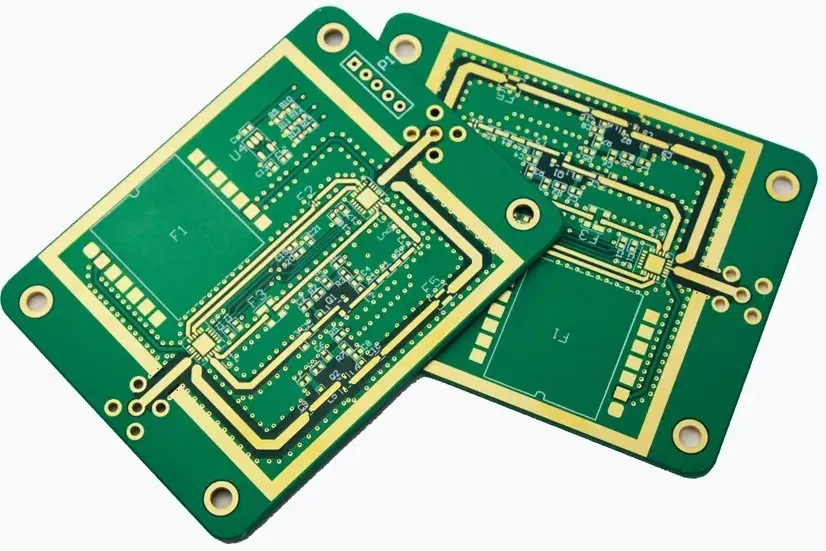
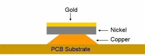
ENIG is a popular surface finish for PCBs, consisting of a thin layer of gold over a thicker layer of nickel. This two-layer coating protects the copper traces from oxidation, provides a flat surface for component assembly, and ensures excellent performance in soldering and wire bonding applications. However, the thickness of each layer—gold and nickel—plays a critical role in determining the board's functionality and cost.
Getting the thickness right is a balancing act. Too thin, and you risk poor solderability or wire bonding failures. Too thick, and you're unnecessarily driving up production costs, especially with gold, which is expensive. By optimizing ENIG thickness, you can achieve reliable performance for your PCBs while managing expenses effectively.
ENIG Gold Thickness Specifications: Finding the Sweet Spot
The gold layer in ENIG serves as a protective barrier against oxidation and enhances solderability. However, gold is costly, so using just the right amount is essential. Industry standards, such as those from the IPC (Institute of Printed Circuits), typically recommend a gold thickness between 0.05 to 0.1 micrometers (μm) for most applications. This range ensures adequate protection and solderability without excessive material use.
For high-reliability applications, such as aerospace or medical devices, a slightly thicker gold layer (up to 0.2 μm) may be specified to ensure durability during multiple reflow cycles. However, exceeding this thickness often provides diminishing returns while significantly increasing costs. For instance, increasing gold thickness from 0.1 μm to 0.2 μm can raise material costs by nearly 50%, depending on the board size and volume.
When specifying gold thickness, consider the end-use of your PCB. If it's for consumer electronics with a single assembly cycle, a thinner layer (0.05 μm) might suffice. For more demanding environments, aim for the higher end of the range, but always evaluate if the performance gain justifies the added expense.
ENIG Nickel Thickness Control: The Foundation of Reliability
The nickel layer in ENIG acts as a barrier between the copper substrate and the gold layer, preventing diffusion and enhancing mechanical strength. Nickel thickness is typically specified between 3 to 6 micrometers (μm) per IPC standards. This range provides a robust foundation for the gold layer and ensures long-term reliability.
Controlling nickel thickness is crucial because deviations can lead to performance issues. If the nickel layer is too thin (below 3 μm), it may not adequately protect the copper, leading to corrosion or "black pad" defects—a condition where the nickel surface oxidizes and causes poor solderability. On the other hand, a nickel layer thicker than 6 μm can introduce stress in the coating, potentially causing cracks or delamination during thermal cycles.
Manufacturers often use process controls like bath chemistry monitoring and plating time adjustments to maintain consistent nickel thickness. Regular testing during production ensures that the layer stays within the desired range, avoiding costly rework or failures in the field.
PCB Surface Finish Thickness Measurement: Ensuring Precision
Accurate measurement of ENIG thickness is vital to confirm that the gold and nickel layers meet specifications. Several non-destructive testing methods are commonly used in the industry to measure these layers with precision.
X-Ray Fluorescence (XRF): This is the most widely used technique for measuring ENIG thickness. XRF analyzers can determine the thickness of both gold and nickel layers by detecting the intensity of X-rays reflected from the surface. This method is fast and accurate, with a typical precision of ±0.01 μm for gold and ±0.1 μm for nickel.
Cross-Sectional Analysis: For more detailed analysis, a small sample of the PCB can be cut and examined under a microscope. This destructive method provides a direct view of the layer thicknesses but is typically used for validation or troubleshooting rather than routine checks due to its invasive nature.
Beta Backscatter: This method is less common but can be used for quick measurements of gold thickness. It relies on the reflection of beta particles to estimate layer depth, though it is less precise than XRF for complex multilayer finishes like ENIG.
Implementing regular thickness measurements during production helps catch deviations early, ensuring consistent quality across batches. For high-volume production, investing in automated XRF systems can save time and reduce human error.
ENIG Thickness and Solderability: Ensuring Strong Connections
Solderability is one of the primary reasons for choosing ENIG as a surface finish. The gold layer provides a clean, oxide-free surface that wets easily with solder, ensuring strong and reliable joints. However, the thickness of both gold and nickel layers directly impacts solderability performance.
A gold layer that is too thin (below 0.05 μm) may not fully protect the nickel underneath, leading to oxidation and poor wetting during soldering. Conversely, an overly thick gold layer (above 0.2 μm) can cause a phenomenon known as "gold embrittlement," where excessive gold dissolves into the solder joint, weakening it. Studies have shown that gold content above 3% by weight in a solder joint can reduce its mechanical strength by up to 20%.
Nickel thickness also plays a role in solderability. A properly controlled nickel layer (3-6 μm) ensures a stable base for soldering, while deviations can lead to defects like black pad, which prevents solder from adhering properly. Maintaining the right ENIG thickness is essential for achieving consistent, high-quality solder joints, especially in fine-pitch components where precision is critical.
ENIG Thickness for Wire Bonding: Meeting High-Reliability Standards
Wire bonding is a common technique in high-reliability applications like automotive and aerospace electronics, where components are directly connected to the PCB using thin wires. ENIG is often chosen for wire bonding due to its flat surface and compatibility with gold or aluminum wires. However, thickness specifications are even more critical in these applications.
For wire bonding, the gold layer should typically be in the range of 0.1 to 0.2 μm to provide a stable surface for bonding. A thinner layer may not offer enough gold for a strong bond, while a thicker layer can lead to inconsistent bonding due to variations in surface hardness. The nickel layer must also be well-controlled (3-6 μm) to provide mechanical support and prevent defects during the bonding process.
In applications requiring multiple wire bonds or exposure to harsh environments, some manufacturers opt for a slightly thicker gold layer to ensure long-term reliability. However, this must be balanced against cost considerations, as even a small increase in gold thickness can significantly impact the budget for large production runs.
Balancing Cost and Performance in ENIG Thickness Optimization
Optimizing ENIG thickness is ultimately about finding the right balance between cost and performance. Gold is the most expensive component of the ENIG finish, so minimizing its thickness without compromising reliability is a priority. For most standard applications, a gold thickness of 0.05 to 0.1 μm paired with a nickel thickness of 3 to 5 μm offers a cost-effective solution with excellent performance.
Here are some practical tips for balancing cost and performance:
- Define Application Requirements: Clearly specify whether your PCB needs to support multiple reflow cycles, wire bonding, or harsh environments. This will guide your thickness specifications.
- Work with Your Manufacturer: Collaborate closely with your PCB supplier to ensure consistent process control and thickness measurement during production.
- Test and Validate: Use sample boards to test solderability and wire bonding performance before committing to full production. This can help identify the optimal thickness for your specific design.
- Consider Alternatives: For less demanding applications, explore other surface finishes like immersion silver or OSP (Organic Solderability Preservative) if ENIG costs are prohibitive.
By tailoring ENIG thickness to your specific needs, you can avoid over-specifying and reduce costs without sacrificing the reliability of your PCBs.
Common Challenges in ENIG Thickness Optimization
While ENIG is a reliable surface finish, achieving optimal thickness can come with challenges. One common issue is inconsistency in plating, where variations in bath chemistry or process parameters lead to uneven gold or nickel layers. This can result in areas of the board with poor solderability or bonding performance.
Another challenge is the risk of black pad defects, often caused by insufficient nickel thickness or contamination during plating. This defect can be mitigated by strict process controls and regular testing of the plating bath.
Finally, cost pressures can tempt manufacturers to cut corners by reducing gold thickness below recommended levels. While this may save money upfront, it often leads to field failures and higher long-term costs due to rework or product recalls. Investing in proper thickness optimization from the start is the best way to avoid these pitfalls.
Conclusion: Achieving Reliable PCBs with Optimized ENIG Thickness
ENIG thickness optimization is a critical factor in producing reliable PCBs that meet performance requirements without unnecessary costs. By focusing on ENIG gold thickness specifications (0.05-0.2 μm) and nickel thickness control (3-6 μm), you can ensure excellent solderability and wire bonding performance for your applications. Accurate PCB surface finish thickness measurement using tools like XRF is essential to maintain consistency, while a clear understanding of how ENIG thickness impacts solderability and wire bonding helps in making informed decisions.
Whether you're designing PCBs for consumer electronics or high-reliability industries, striking the right balance between cost and performance is achievable with careful planning and collaboration with your manufacturing partner. Optimized ENIG thickness not only enhances the durability and functionality of your boards but also ensures you get the best value for your investment.