In the fast-paced world of video processing, designing high-speed printed circuit boards (PCBs) is critical to ensure clear, uninterrupted signals. Whether you're working on a camera system, video streaming device, or high-definition display, signal degradation can ruin performance. So, how do you design a high-speed PCB layout for video processing while minimizing signal loss? The key lies in focusing on signal integrity, impedance control, crosstalk reduction, and managing signal attenuation.
In this comprehensive guide, we'll dive deep into the essentials of designing high-speed video processing PCBs. From understanding signal integrity in video PCBs to practical tips for impedance control and crosstalk reduction, this post will equip you with the knowledge to tackle signal degradation head-on. Let’s explore how to optimize your PCB designs for top-notch video performance.
Why Signal Degradation Matters in High-Speed Video Processing PCBs
Video processing systems often handle data rates exceeding several gigabits per second (Gbps). At these speeds, even minor issues like signal reflection, crosstalk, or attenuation can distort video output, causing pixel errors, jitter, or complete signal failure. Signal degradation directly impacts the quality of video streams, leading to delays or loss of data in real-time applications.
For engineers working on high-speed PCB layouts for video applications, maintaining signal integrity is non-negotiable. A poorly designed PCB can introduce noise, reduce clarity, and even damage components over time. By focusing on key design principles, such as impedance matching and proper trace routing, you can minimize these risks and ensure reliable performance.
Understanding Signal Integrity in Video PCBs
Signal integrity refers to the quality of an electrical signal as it travels from the transmitter to the receiver across a PCB. In video PCBs, where data rates can reach 5 Gbps or higher (as seen in HDMI 2.0 or DisplayPort standards), maintaining signal integrity is a challenge. Issues like reflections, noise, and timing errors can degrade the signal, leading to blurry images or dropped frames.
To achieve optimal signal integrity in video PCBs, consider the following factors:
- Trace Length Matching: Ensure that signal traces carrying differential pairs (common in video interfaces like HDMI) are of equal length to avoid timing skew. A mismatch as small as 10 mils can introduce delays at high frequencies.
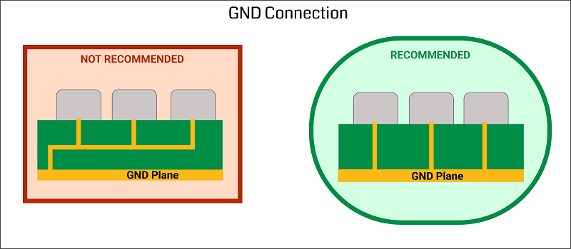
- Ground Planes: Use continuous ground planes to provide a low-impedance return path for signals. Gaps or splits in the ground plane can cause signal loops, increasing noise.
- Termination Resistors: Add termination resistors at the end of high-speed traces to prevent reflections. For instance, a 50-ohm termination is standard for many high-speed video signals.
Impedance Control in PCB Video Design
Impedance control is a cornerstone of high-speed PCB design, especially for video applications. Impedance mismatches can cause signal reflections, leading to data errors. For video PCBs handling signals like HDMI or MIPI, maintaining a consistent impedance—often 50 ohms for single-ended traces or 100 ohms for differential pairs—is crucial.
Here’s how to achieve proper impedance control in PCB video design:
- Calculate Trace Width and Spacing: Use impedance calculators or simulation tools to determine the correct trace width and spacing based on your PCB stack-up and dielectric material. For example, a 4-layer PCB with FR-4 material (dielectric constant of 4.2) might require a trace width of 6 mils for a 50-ohm impedance.
- Choose the Right Materials: High-frequency signals in video PCBs benefit from low-loss materials with a lower dielectric constant (Dk). Materials with a Dk of 3.5 or lower can reduce signal loss compared to standard FR-4.
- Control Layer Stack-Up: Design your PCB stack-up to maintain consistent impedance across layers. Keep signal layers close to reference planes (ground or power) to minimize variations.
By prioritizing impedance control, you ensure that signals travel without distortion, preserving video quality even at high data rates.
Crosstalk Reduction in Video PCB Layouts
Crosstalk occurs when signals from adjacent traces interfere with each other, a common issue in densely packed video PCB layouts. This interference can introduce noise, distorting video signals and causing errors in data transmission. Crosstalk reduction in video PCBs is essential for maintaining clean, reliable signals.
Follow these strategies to minimize crosstalk:
- Increase Trace Spacing: Maintain at least 3x the trace width as spacing between high-speed traces. For a 5-mil trace, aim for a 15-mil gap to reduce electromagnetic coupling.
- Use Guard Traces: Place grounded guard traces between sensitive high-speed lines to act as a shield. Connect these traces to the ground plane with vias at regular intervals (every 0.5 inches or less).
- Route Signals on Different Layers: If space is limited, route high-speed video signals on separate layers, with a ground plane between them to block interference.
Implementing these techniques can significantly lower crosstalk, ensuring that video signals remain clear even in compact designs.
Signal Attenuation in Video PCBs: Causes and Solutions
Signal attenuation refers to the loss of signal strength as it travels through a PCB trace. In video PCBs, attenuation can degrade high-frequency signals, resulting in poor video quality or data loss. Attenuation is influenced by factors like trace length, material properties, and frequency.
Common causes of signal attenuation in video PCBs include:
- Dielectric Loss: The PCB substrate absorbs energy from high-frequency signals, reducing their amplitude. Standard FR-4 material can cause significant loss at frequencies above 1 GHz.
- Conductor Loss: Resistance in copper traces leads to signal loss, especially in long traces or at high frequencies where the skin effect limits current flow to the surface of the conductor.
- Trace Length: Longer traces increase resistance and dielectric loss, amplifying attenuation. For instance, a 10-inch trace can cause noticeable signal loss at 5 Gbps.
To combat signal attenuation, consider these solutions:
- Shorten Trace Lengths: Keep high-speed video signal traces as short as possible. If long traces are unavoidable, use repeaters or amplifiers to boost the signal.
- Use Low-Loss Materials: Opt for substrates with low dissipation factor (Df) values, such as Rogers or Isola materials, which can reduce dielectric loss by up to 50% compared to FR-4 at high frequencies.
- Wider Traces: Increase trace width to lower conductor resistance, though balance this with impedance requirements. A wider trace can reduce loss but may alter impedance if not calculated properly.
By addressing signal attenuation in video PCBs, you can maintain signal strength over longer distances, ensuring high-quality video output.
Practical Tips for High-Speed PCB Layout in Video Applications
Designing a high-speed PCB layout for video processing requires attention to detail and adherence to best practices. Here are actionable tips to guide your design process:
- Differential Pair Routing: Route differential pairs (used in standards like HDMI and DisplayPort) with consistent spacing and length matching. Avoid sharp bends—use 45-degree angles or curves to maintain signal integrity.
- Via Optimization: Minimize the use of vias in high-speed signal paths, as they introduce inductance and capacitance. If vias are necessary, use back-drilling to remove unused via stubs, reducing signal reflections.
- Power Delivery Network (PDN): Design a robust PDN to provide stable power to high-speed components. Place decoupling capacitors close to IC pins (within 0.1 inches) to filter noise, using values like 0.1 μF for high-frequency noise suppression.
- Simulation Tools: Use simulation software to analyze signal integrity, impedance, and crosstalk before fabrication. Tools can predict issues like reflections or attenuation, saving time and cost during prototyping.
Applying these practices to your high-speed PCB layout can prevent common pitfalls and enhance video processing performance.
Advanced Techniques for Minimizing Signal Degradation
For cutting-edge video applications pushing data rates beyond 10 Gbps, advanced design techniques become essential. These methods address extreme signal degradation challenges:
- Equalization: Implement pre-emphasis or equalization circuits at the transmitter or receiver to compensate for signal loss over long traces. This technique boosts high-frequency components to counteract attenuation.
- Backplane Design: For systems using multiple PCBs connected via backplanes, ensure controlled impedance across connectors and use low-loss materials to maintain signal quality.
- Electromagnetic Interference (EMI) Shielding: Enclose sensitive video signal traces with grounded copper pours or shielding cans to block external EMI, which can degrade signal quality at high frequencies.
These advanced strategies can make a significant difference in high-performance video systems where every bit of signal quality counts.
Conclusion: Building Reliable High-Speed Video Processing PCBs
Designing high-speed video processing PCBs is a complex task, but by focusing on signal integrity, impedance control, crosstalk reduction, and signal attenuation, you can minimize signal degradation effectively. Start with a solid understanding of your design requirements, such as data rates and video standards, then apply best practices like trace length matching, proper material selection, and optimized routing.
Every detail matters in high-speed PCB layouts for video applications. From choosing the right substrate to simulating your design before production, a methodical approach ensures that your PCB delivers crisp, reliable video output. With the tips and techniques outlined in this guide, you're well-equipped to tackle the challenges of high-speed video PCB design and achieve outstanding results.
At ALLPCB, we’re committed to supporting engineers with the tools and expertise needed for cutting-edge PCB designs. Whether you're working on a compact video streaming device or a large-scale display system, mastering these design principles will help you create boards that perform flawlessly under demanding conditions.
 ALLPCB


