 ALLPCB


Designing printed circuit boards (PCBs) for ultrasound applications is a complex task that requires careful component selection to ensure optimal performance. If you're searching for guidance on PCB component selection for ultrasound, you're in the right place. This guide provides a detailed overview of the critical criteria for choosing components like high frequency components for PCBs, low noise amplifiers for PCBs, ADC selection for PCBs, and transducer drivers for PCBs. We'll dive into the specifics to help you build reliable and efficient ultrasound systems.
Ultrasound technology, widely used in medical imaging, industrial testing, and other fields, relies on high-frequency sound waves to create images or detect objects. The PCB at the heart of these systems must handle high-frequency signals, minimize noise, and ensure precise data conversion. Let's explore the key considerations for selecting components to meet these demanding requirements.
Why Component Selection Matters in Ultrasound PCBs
In ultrasound systems, every component on the PCB plays a vital role in signal integrity, accuracy, and overall performance. Poor component choices can lead to signal distortion, high noise levels, or inefficient power use, which can compromise the quality of ultrasound imaging or measurement. By focusing on the right criteria for PCB component selection in ultrasound, you can avoid costly redesigns and ensure your system meets industry standards.
The main challenges in ultrasound PCB design include handling frequencies often ranging from 1 MHz to 20 MHz, maintaining low noise for clear signal detection, and ensuring compatibility between components like transducers, amplifiers, and analog-to-digital converters (ADCs). Let's break down the selection criteria for each key component category.
1. High Frequency Components for PCBs: Handling Ultrasound Signals
Ultrasound systems operate at high frequencies, which means the components on your PCB must be capable of processing these signals without loss or distortion. When selecting high frequency components for PCBs, consider the following factors:
- Frequency Range Compatibility: Ensure that components like capacitors, inductors, and resistors are rated for the specific frequency range of your ultrasound system. For example, a typical medical ultrasound device may operate at 5-10 MHz, so choose components with minimal parasitic effects at these frequencies.
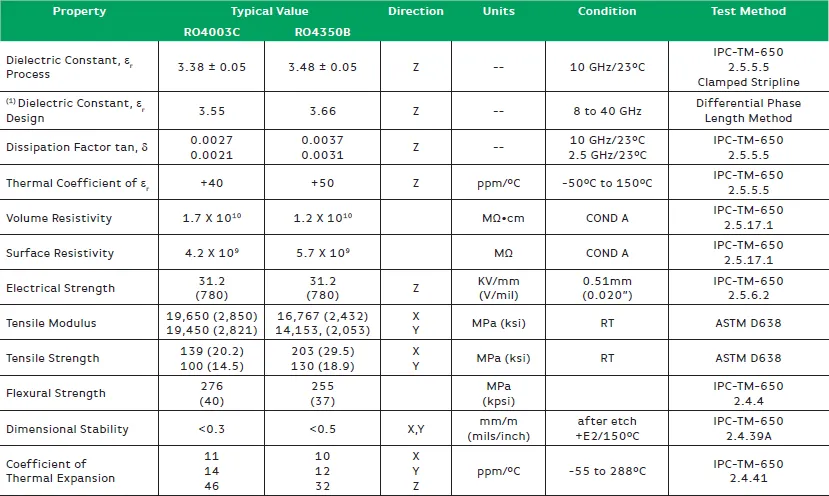
- Material Selection: Use PCB substrates designed for high-frequency applications, such as those with low dielectric loss. Materials with a dielectric constant (Dk) of around 3.5 or lower are often preferred to reduce signal attenuation.
- Signal Integrity: High-frequency signals are prone to interference and crosstalk. Opt for components with tight tolerances and low equivalent series resistance (ESR) to maintain signal quality.
2. Low Noise Amplifiers for PCBs: Ensuring Clear Signal Amplification
Ultrasound signals are often very weak, especially after traveling through tissues or materials. Amplifiers are used to boost these signals, but they must do so without introducing noise. When choosing low noise amplifiers for PCBs, keep these criteria in mind:
- Noise Figure (NF): Look for amplifiers with a low noise figure, ideally below 2 dB, to minimize added noise during signal amplification. A lower NF ensures better signal-to-noise ratio (SNR), critical for clear ultrasound imaging.
- Gain and Bandwidth: Select an amplifier with sufficient gain (often 20-40 dB) and a bandwidth that covers your operating frequency range. For instance, if your system operates at 10 MHz, the amplifier must support this frequency without roll-off.
- Power Consumption: Ultrasound devices, especially portable ones, require energy-efficient components. Choose amplifiers with low quiescent current to extend battery life without sacrificing performance.
- Layout Considerations: Place amplifiers close to the signal source on the PCB to reduce noise pickup from long traces. Use proper grounding and shielding techniques to further minimize interference.
3. ADC Selection for PCBs: Converting Analog Signals to Digital Data
Analog-to-digital converters (ADCs) are crucial in ultrasound systems for converting amplified analog signals into digital data for processing. Proper ADC selection for PCBs can significantly impact the resolution and accuracy of your ultrasound images. Consider these factors:
- Sampling Rate: The ADC must sample at a rate at least twice the highest frequency of the ultrasound signal (Nyquist rate). For a 10 MHz signal, choose an ADC with a sampling rate of 20 MSPS (mega samples per second) or higher to capture the signal accurately.
- Resolution: Higher resolution ADCs, such as 12-bit or 14-bit, provide better detail in ultrasound images by distinguishing smaller signal variations. However, balance resolution with cost and processing speed.
- Input Range and Noise: Ensure the ADC's input voltage range matches the output of your amplifier. Also, select an ADC with low input-referred noise to avoid degrading the SNR achieved by your low noise amplifier.
- Power Efficiency: Like other components, ADCs in portable ultrasound devices should consume minimal power. Look for low-power or power-scalable ADCs that adjust consumption based on sampling rate.
4. Transducer Drivers for PCBs: Powering the Ultrasound Source
Transducer drivers are responsible for generating the electrical pulses that excite the ultrasound transducer to produce sound waves. Selecting the right transducer drivers for PCBs is essential for efficient energy transfer and high-quality signal generation. Key criteria include:
- Voltage and Current Capability: Ultrasound transducers often require high-voltage pulses (50-200 V) to generate sufficient acoustic energy. Choose drivers that can deliver these voltages with fast rise times (e.g., less than 10 ns) for sharp, clear pulses.
- Switching Speed: High switching speeds are necessary to produce short-duration pulses, which improve the resolution of ultrasound images. Look for drivers with fast turn-on and turn-off times.
- Thermal Management: High-voltage drivers can generate significant heat. Ensure the driver components are rated for the expected power dissipation and incorporate heat sinks or thermal vias in your PCB design if needed.
- Matching Impedance: Match the driver's output impedance to the transducer's input impedance to maximize power transfer and minimize signal reflections. For example, if the transducer has an impedance of 50 ohms, the driver should be designed or selected to match this value.
5. General PCB Design Tips for Ultrasound Applications
Beyond individual component selection, the overall PCB design plays a critical role in the performance of ultrasound systems. Here are some additional tips to ensure success:
- Layer Stackup: Use a multilayer PCB with dedicated ground and power planes to reduce noise and improve signal integrity. A 4-layer or 6-layer design is often suitable for ultrasound applications, allowing separation of analog and digital signals.
- Trace Routing: Keep high-frequency signal traces short and direct to minimize parasitic capacitance and inductance. Use controlled impedance traces for critical paths to maintain signal fidelity.
- Decoupling and Filtering: Place decoupling capacitors close to power pins of active components like amplifiers and ADCs to filter out noise. Use ferrite beads or low-pass filters to further clean power supplies.
- Shielding: Incorporate shielding techniques, such as grounded copper pours or metal enclosures, to protect sensitive analog circuits from electromagnetic interference (EMI).
Balancing Performance, Cost, and Size in Ultrasound PCB Design
While performance is paramount, practical constraints like cost and board size often influence component selection. High-performance components, such as ADCs with ultra-high sampling rates or amplifiers with extremely low noise figures, can be expensive. Evaluate whether the incremental performance gain justifies the cost for your specific application. Similarly, smaller components may save space on the PCB but could be harder to assemble or less reliable under high-voltage conditions.
For portable ultrasound devices, prioritize compact, low-power components to fit within tight space and energy constraints. In contrast, for stationary equipment, you might focus more on maximizing performance over size or power efficiency. Always define your project requirements—such as target resolution, imaging depth, or battery life—before finalizing component choices.
Testing and Validation of Ultrasound PCBs
Once you've selected components and designed your PCB, thorough testing is essential to validate performance. Use oscilloscopes to measure signal integrity at key points, such as the output of the transducer driver and the input to the ADC. Check for noise levels, distortion, and timing issues that could affect image quality. Additionally, perform thermal imaging to identify hot spots on the board that might indicate inefficient components or poor layout design.
Simulate real-world conditions by testing the PCB with the actual transducer and under varying loads. This ensures that the system can handle the dynamic range of signals encountered in practical use. Iterative testing and tweaking of component values or layout may be necessary to achieve optimal results.
Conclusion: Building Better Ultrasound PCBs with Smart Component Choices
Designing PCBs for ultrasound systems is a challenging yet rewarding endeavor. By focusing on the right criteria for PCB component selection in ultrasound, including choosing appropriate high frequency components for PCBs, low noise amplifiers for PCBs, ADC selection for PCBs, and transducer drivers for PCBs, you can create systems that deliver high-quality imaging or precise measurements.
Remember to prioritize signal integrity, minimize noise, and match components to the specific frequency and power requirements of your application. With careful planning, thoughtful design, and rigorous testing, your ultrasound PCB can meet the demands of modern medical, industrial, or research applications. Trust in a reliable manufacturing partner to bring your design to life with precision and quality, ensuring that every component performs as intended in the final product.


