 ALLPCB


In the fast-evolving world of electronics, high-density PCB designs are becoming the norm as devices get smaller and more complex. One often-overlooked aspect of these designs is the silkscreen layer, which plays a critical role in assembly, testing, and troubleshooting. So, how do you optimize silk screen resolution for high-density PCB designs with fine-pitch components? The key lies in adhering to silkscreen design rules for HDI (High-Density Interconnect) boards, focusing on minimum line widths, and ensuring clarity without clutter. In this comprehensive guide, we’ll dive deep into the best practices for silkscreen optimization, tailored for engineers working on intricate layouts.
Why Silkscreen Matters in High-Density PCB Designs
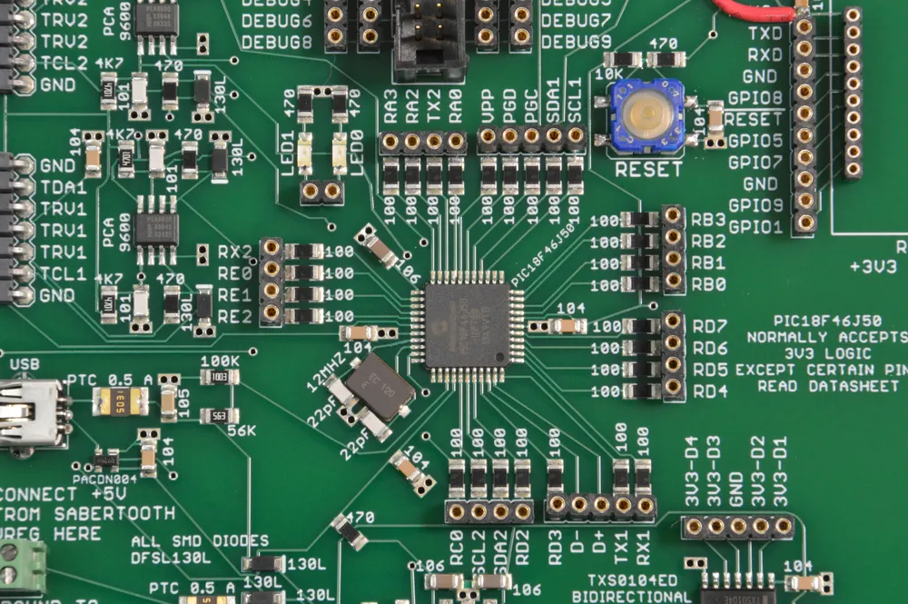
Silkscreen, the printed layer of text and symbols on a PCB, acts as a roadmap for assembly and maintenance. For high-density PCB designs, where components are packed tightly and fine-pitch components (with lead spacing as small as 0.5mm or less) dominate, a poorly optimized silkscreen can lead to assembly errors or misinterpretations. Clear markings ensure that technicians can identify components, polarities, and test points without confusion, even on boards with hundreds of parts per square inch.
Optimizing silkscreen resolution is not just about aesthetics; it’s about functionality. High-density interconnect (HDI) boards often feature microvias, blind vias, and multiple layers (sometimes exceeding 20), making accurate labeling essential for debugging signal integrity issues or power distribution faults. Let’s explore how to achieve this precision.
Understanding Silkscreen Design Rules for HDI Boards
When designing silkscreen for HDI boards, following strict guidelines ensures that markings remain legible and useful. Here are the core silkscreen design rules tailored for high-density layouts:
- Minimum Line Width: The silkscreen minimum line width is a critical parameter. Most manufacturers recommend a minimum of 0.15mm (6 mils) for line thickness to ensure readability under standard printing processes. For ultra-dense designs, pushing this to 0.1mm (4 mils) might be possible with advanced printing techniques, but always confirm with your fabrication house.
- Text Height: Text should be at least 1.5mm (60 mils) tall for visibility. For extremely compact areas near fine-pitch components, reducing this to 1mm (40 mils) can work if high-resolution printing is available.
- Clearance from Pads and Vias: Maintain a clearance of at least 0.2mm (8 mils) between silkscreen markings and solder pads or vias to prevent ink from interfering with soldering or causing shorts during assembly.
- Avoid Overcrowding: In high-density designs, space is limited. Prioritize essential markings like component designators and polarity indicators over non-critical labels to avoid clutter.
These rules are not arbitrary; they stem from the limitations of silkscreen printing technology and the need for precision in HDI layouts. For instance, a line width below 0.1mm risks becoming illegible due to ink spread or printing inaccuracies, especially on boards with surface finishes like ENIG (Electroless Nickel Immersion Gold).
Challenges with Fine-Pitch Components and Silkscreen
Fine-pitch components, such as QFN (Quad Flat No-Lead) packages or BGA (Ball Grid Array) chips with pitches below 0.8mm, pose unique challenges for silkscreen design. The limited space around these components means there’s little room for detailed markings. Here’s how to address these issues:
- Minimalist Markings: Use simple symbols (like a dot for pin 1 or an arrow for orientation) instead of full text labels near fine-pitch parts. This saves space while still conveying critical information.
- Offset Labels: If space is too tight, place designators slightly away from the component, connected by a small line or arrow to indicate the association.
- Layered Information: For complex boards, consider using both top and bottom silkscreen layers to distribute information, especially if components are mounted on both sides.
The goal is to balance clarity with space constraints. For example, on a board with a 0.5mm pitch BGA, placing a full “U1” label directly next to the part might overlap with nearby traces or vias. Instead, a small “1” near pin 1, combined with a reference elsewhere on the board, can be more effective.
Optimizing Silkscreen Resolution for Clarity
Silkscreen resolution refers to the precision and sharpness of printed markings on the PCB. Higher resolution is crucial for high-density designs where every millimeter counts. Here are actionable tips to optimize resolution:
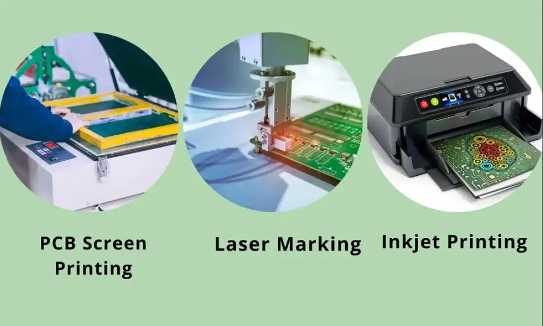
- Choose the Right Printing Method: Traditional silkscreen printing offers resolutions suitable for line widths down to 0.15mm. For finer details, consider digital inkjet printing, which can achieve resolutions supporting line widths as small as 0.1mm with greater accuracy.
- Select High-Contrast Colors: White ink on dark solder masks (like green or black) provides the best readability. Avoid low-contrast combinations like yellow on green, especially for small text on HDI boards.
- Work with Fabrication Limits: Always review the capabilities of your manufacturing partner. Some can handle ultra-fine silkscreen resolutions, while others may struggle with anything below 0.2mm line width.
- Use Vector-Based Graphics: Design silkscreen layers using vector graphics in your PCB software to ensure sharp, scalable markings without pixelation, even at small sizes.
By focusing on resolution, you can ensure that even the tiniest markings remain legible under a magnifying glass during assembly or inspection. This is particularly important for boards with fine-pitch components where a single misplaced part can cause signal integrity issues, such as crosstalk or impedance mismatches in high-speed designs operating at frequencies above 1 GHz.
Best Practices for Silkscreen in High-Density Interconnect (HDI) Designs
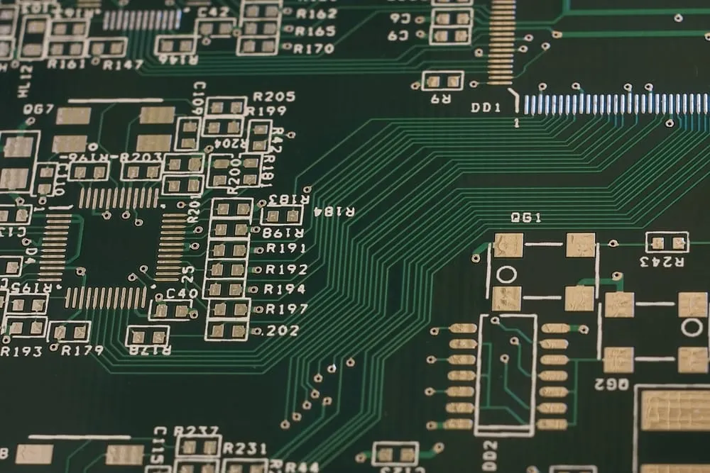
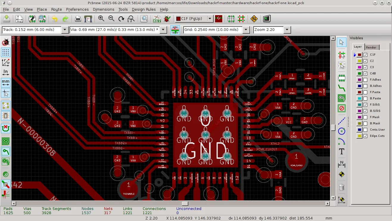
HDI boards often incorporate microvias (diameters as small as 0.1mm) and stacked layers, making silkscreen optimization even more critical. Here are tailored best practices for HDI silkscreen design:
- Prioritize Test Points and Vias: Clearly label test points and critical vias with small, precise markings. For example, use “TP1” for test point 1 near a via connected to a 3.3V power rail to aid in debugging.
- Account for Layer Stacking: In multi-layer HDI designs, indicate which layer a marking refers to if relevant, such as “GND-L2” for a ground connection on layer 2.
- Minimize Silkscreen on Inner Layers: While inner layers don’t typically have silkscreen, some advanced designs may include markings for buried components. Keep these minimal to avoid fabrication complexity.
- Coordinate with Assembly Teams: Ensure your silkscreen design aligns with the needs of the assembly team. For instance, clearly mark polarity for diodes or capacitors near fine-pitch ICs to prevent reverse installations.
Implementing these practices can significantly reduce errors during the production of HDI boards, where a single misstep can lead to costly rework. For example, mislabeling a microvia connected to a high-speed signal line (with impedance controlled at 50 ohms) could result in hours of troubleshooting.
Tools and Software for Silkscreen Optimization
Modern PCB design software offers robust tools to help optimize silkscreen for high-density layouts. Here are some features to leverage:
- Automated Design Rule Checks (DRC): Use DRC features to enforce silkscreen minimum line width and clearance rules automatically, catching errors before fabrication.
- Layer Management: Organize silkscreen layers separately from other design elements to fine-tune placement and visibility without affecting traces or pads.
- Preview Modes: Utilize 3D preview modes to visualize how silkscreen will appear on the final board, especially near fine-pitch components or dense areas.
By integrating these tools into your workflow, you can streamline the design process and ensure that silkscreen markings meet both aesthetic and functional requirements for HDI boards.
Common Mistakes to Avoid in Silkscreen Design
Even experienced engineers can make errors when optimizing silkscreen for high-density PCB designs. Here are pitfalls to watch out for:
- Ignoring Manufacturer Guidelines: Failing to check fabrication capabilities can result in illegible markings if the printer can’t handle fine line widths below 0.15mm.
- Overloading with Information: Too many labels in a small area can create visual noise, making it hard to identify critical components during assembly.
- Placing Markings Under Components: Avoid putting silkscreen text or symbols under parts like BGAs where they’ll be hidden after assembly.
- Neglecting Font Size: Text smaller than 1mm in height risks becoming unreadable, especially on boards inspected without magnification.
Avoiding these mistakes ensures that your silkscreen remains a helpful tool rather than a source of confusion during production or maintenance.
Conclusion: Elevating Your High-Density PCB Designs with Silkscreen Optimization
Optimizing silk screen resolution for high-density PCB designs is a crucial step in ensuring the success of modern electronics projects. By adhering to silkscreen design rules for HDI, focusing on minimum line widths, and addressing the unique challenges of fine-pitch components, you can create boards that are not only functional but also easy to assemble and maintain. Whether you’re working on a compact IoT device or a multi-layer server board, a well-designed silkscreen layer can save time, reduce errors, and improve overall quality.
Start by reviewing your current silkscreen practices against the guidelines shared here. Focus on clarity, precision, and collaboration with your fabrication and assembly teams to achieve the best results. With these strategies, you’ll be well-equipped to tackle the complexities of high-density interconnect designs and beyond.


