 ALLPCB


If you're searching for cutting-edge solutions in PCB design, particularly for high-density applications, you've likely come across terms like HDI PCB, Rogers HDI PCB, and high density interconnector PCBs. So, what makes Rogers materials and advanced fabrication techniques stand out for high-density designs? Simply put, Rogers PCB materials offer superior electrical performance and thermal stability, making them ideal for complex, high-speed, and compact designs. In this blog, we dive deep into the advanced fabrication techniques used to create Rogers HDI PCBs, exploring how they meet the demands of modern electronics.
What Are High-Density Interconnect (HDI) PCBs?
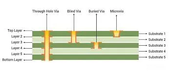
High-Density Interconnect (HDI) PCBs are a type of printed circuit board designed to pack more components into a smaller space. Unlike traditional PCBs, HDI boards feature finer lines, smaller vias, and higher layer counts. This allows for greater functionality in compact devices like smartphones, medical equipment, and aerospace systems. The use of microvias, blind vias, and buried vias in HDI PCBs enables intricate routing and improved signal integrity, which are critical for high-speed applications.
When combined with Rogers materials—known for their low dielectric constant and excellent thermal management—HDI PCBs become even more powerful. Rogers HDI PCBs are often the go-to choice for engineers working on RF, microwave, and high-frequency designs where performance cannot be compromised.
Why Choose Rogers Materials for HDI PCBs?
Rogers materials are a class of high-performance laminates specifically engineered for demanding applications. Unlike standard FR-4 materials, Rogers laminates offer several advantages that make them ideal for high density interconnector PCBs:
- Low Dielectric Constant (Dk): Rogers materials typically have a Dk ranging from 2.2 to 10.2, reducing signal loss and crosstalk in high-frequency designs.
- Low Loss Tangent: With loss tangents as low as 0.0009 at 10 GHz, these materials ensure minimal energy dissipation, critical for RF and microwave applications.
- Thermal Stability: Rogers laminates can withstand temperatures up to 280°C without degrading, making them suitable for harsh environments.
- Controlled Impedance: These materials provide consistent impedance values (e.g., 50 ohms for RF designs), ensuring reliable signal transmission.
For high-density designs, where space is limited and signal integrity is paramount, Rogers materials provide the foundation for success. Their ability to maintain performance in compact, multilayer HDI PCBs makes them a preferred choice for industries like telecommunications and automotive electronics.
Advanced Fabrication Techniques for Rogers HDI PCBs
Fabricating HDI PCBs with Rogers materials requires precision and expertise due to the complexity of high-density designs and the unique properties of the laminates. Below, we explore the advanced techniques used to achieve optimal results in Rogers HDI PCB production.
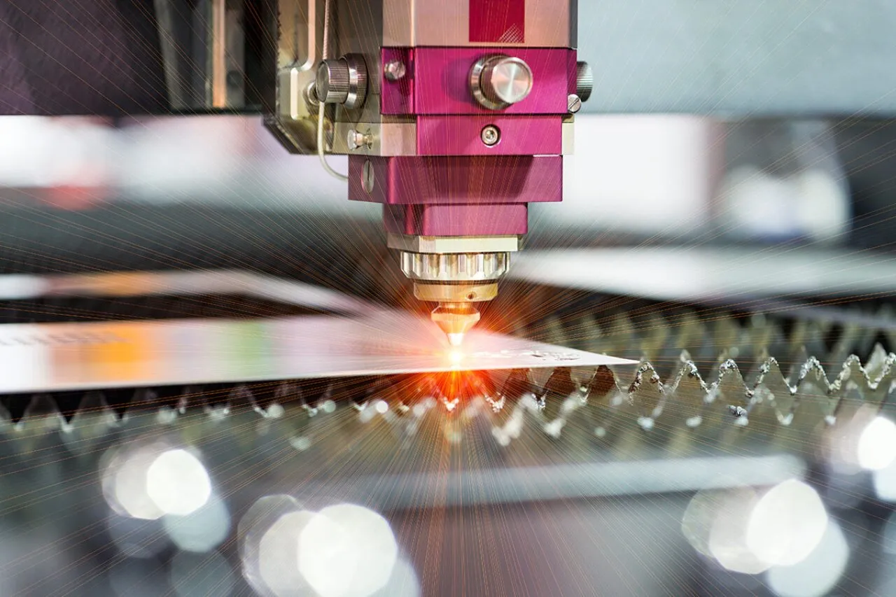
1. Laser Drilling for Microvias
Microvias are tiny holes (typically less than 150 microns in diameter) that connect layers in an HDI PCB. Traditional mechanical drilling isn’t precise enough for these small features, so laser drilling is used instead. This technique employs a focused laser beam to create clean, accurate microvias with minimal damage to surrounding materials.
For Rogers HDI PCBs, laser drilling is especially important because the materials often have different thermal and mechanical properties compared to standard laminates. The process must be carefully controlled to avoid overheating or delamination. Modern laser drilling systems can achieve aspect ratios of up to 1:1, ensuring reliable connections even in dense, multilayer boards.
2. Sequential Build-Up (SBU) Technology
Sequential Build-Up (SBU) is a fabrication method used to create multilayer HDI PCBs by adding layers one at a time. This technique allows for the integration of microvias, blind vias, and buried vias at different stages of the build process, maximizing density and flexibility in design.
When working with Rogers materials, SBU technology ensures that each layer is precisely aligned and bonded under controlled conditions. This is critical because Rogers laminates often have lower coefficients of thermal expansion (CTE) compared to FR-4, requiring specialized handling to prevent warping or misalignment during lamination. SBU can support layer counts of 14 or more, enabling highly complex high density interconnector PCBs for advanced applications.
3. Fine-Line Etching for High-Density Traces
In HDI designs, trace widths and spacing can be as small as 50 microns or less. Achieving these fine lines on Rogers materials requires advanced etching techniques that ensure precision without undercutting or damaging the substrate. Photolithography, combined with high-resolution imaging, is often used to define these narrow traces and spaces.
Rogers materials, with their smooth surface and consistent dielectric properties, support finer lines with better signal integrity. For example, in a high-frequency design operating at 5 GHz, traces on a Rogers HDI PCB can maintain impedance control within ±5%, reducing signal reflection and loss compared to standard materials.
4. Controlled Impedance Routing
High-speed designs demand strict control over impedance to prevent signal distortion. Rogers materials are inherently suited for controlled impedance due to their stable dielectric properties. During fabrication, advanced simulation tools are used to calculate trace widths, spacing, and layer stack-ups to achieve target impedance values, such as 50 ohms or 100 ohms for differential pairs.
In Rogers HDI PCBs, impedance control is further enhanced by minimizing via stubs and optimizing layer transitions. This ensures that signals travel at consistent speeds—often exceeding 10 Gbps—without interference, making these boards ideal for applications like 5G infrastructure and high-speed data transfer.
5. Advanced Surface Finishes for Reliability
The surface finish of an HDI PCB affects its solderability, durability, and performance. For Rogers HDI PCBs used in high-density designs, advanced finishes like Electroless Nickel Immersion Gold (ENIG) or Immersion Silver are often applied. These finishes provide a flat, uniform surface for fine-pitch components and protect against oxidation.
ENIG, for instance, offers excellent corrosion resistance and can support multiple reflow cycles without degrading, which is essential for the high thermal demands of Rogers-based boards. This ensures long-term reliability in applications where high density interconnector PCBs are exposed to harsh conditions.
Challenges in Fabricating Rogers HDI PCBs
While Rogers materials and HDI designs offer unmatched performance, they come with unique fabrication challenges. Understanding these hurdles is key to ensuring a successful outcome for high-density projects.
- Material Handling: Rogers laminates are more sensitive to moisture and temperature changes than standard materials. Improper storage or processing can lead to defects like delamination or cracking.
- Cost Considerations: High-performance materials and advanced techniques like laser drilling increase production costs. However, the improved performance often justifies the investment for critical applications.
- Design Complexity: The dense routing and multilayer structures of HDI PCBs require meticulous planning and simulation to avoid signal integrity issues or manufacturing errors.
Partnering with an experienced fabrication team can help overcome these challenges, ensuring that your Rogers HDI PCB meets the highest standards of quality and performance.
Applications of Rogers HDI PCBs in High-Density Designs
The combination of Rogers materials and HDI technology opens up a wide range of possibilities for compact, high-performance electronics. Here are some key areas where these boards excel:
- Telecommunications: Rogers HDI PCBs are widely used in 5G base stations and antennas, where low signal loss and high-frequency performance are critical.
- Aerospace and Defense: These boards support radar systems and communication devices, offering reliability in extreme environments with temperatures ranging from -55°C to 125°C.
- Medical Devices: Compact HDI designs with Rogers materials are ideal for wearable health monitors and imaging equipment, where space and precision are paramount.
- Automotive Electronics: Advanced driver-assistance systems (ADAS) and infotainment systems benefit from the high-speed signal transmission and thermal stability of Rogers HDI PCBs.
Best Practices for Designing Rogers HDI PCBs
To maximize the benefits of Rogers materials in high-density designs, engineers should follow these best practices during the design and fabrication stages:
- Optimize Layer Stack-Up: Plan the layer configuration to balance signal integrity and thermal management. For example, place high-speed signals on inner layers to reduce interference.
- Use Simulation Tools: Employ advanced software to simulate impedance, signal loss, and thermal behavior before fabrication. This helps identify potential issues early.
- Minimize Via Stubs: Design vias to avoid stubs, which can cause signal reflections in high-frequency applications.
- Collaborate with Fabricators: Work closely with your manufacturing team to ensure that design specifications align with fabrication capabilities, especially when using specialized materials like Rogers laminates.
Conclusion: Elevating High-Density Designs with Rogers HDI PCBs
In the world of modern electronics, where devices are becoming smaller and more powerful, high density interconnector PCBs are essential. By leveraging Rogers materials and advanced fabrication techniques like laser drilling, sequential build-up, and fine-line etching, engineers can create HDI PCBs that deliver exceptional performance in the most demanding applications.
Whether you're working on telecommunications infrastructure, aerospace systems, or medical devices, Rogers HDI PCBs provide the reliability, signal integrity, and thermal stability needed to push the boundaries of innovation. With careful design and precision manufacturing, these boards can help you achieve unparalleled results in high-density designs.
At ALLPCB, we specialize in delivering high-quality Rogers HDI PCB solutions tailored to your specific needs. Our expertise in advanced fabrication ensures that your projects benefit from the latest technologies and best practices, bringing your ideas to life with precision and efficiency.


