ALLPCB


In the fast-paced world of printed circuit board (PCB) design, precision is everything. Gerber files, the industry-standard format for PCB fabrication, act as the blueprint that bridges your design to the final product. However, even a minor error in these files can lead to costly manufacturing delays or defective boards. Gerber file viewers are essential tools that allow engineers to inspect and verify these files before sending them to manufacturers, ensuring error-free production. In this blog, we explore how Gerber file viewers work, why they're critical for PCB fabrication, and how to use them effectively to catch issues early.
Whether you're designing a simple two-layer board or a complex high-density interconnect (HDI) PCB, understanding how to leverage Gerber viewers can save time, reduce costs, and improve the quality of your boards. Let's dive into the details of these tools and share practical tips to optimize your PCB fabrication process.
What Are Gerber Files and Why Do They Matter?
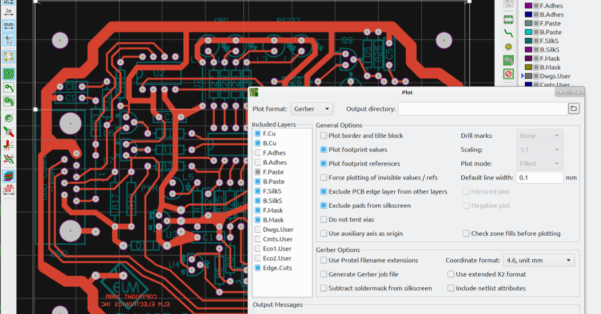
Gerber files are ASCII vector format files that contain layer-by-layer data for PCB fabrication, including copper traces, solder masks, silkscreens, and drill patterns. Developed in the 1960s by Gerber Systems Corporation, the format has evolved into the RS-274X standard, which supports embedded metadata for precise manufacturing instructions. Each Gerber file corresponds to a specific layer of the PCB, such as the top copper layer or bottom solder mask, while drill files (often in Excellon format) specify hole locations and sizes.
These files are critical because they communicate your design intent to the manufacturer. Errors like misaligned layers, incorrect trace widths, or missing drill holes can result in boards that fail to meet electrical or mechanical requirements. For example, a 0.1 mm misalignment in a high-speed PCB could alter impedance, potentially causing signal integrity issues at frequencies above 1 GHz. Gerber viewers help you spot these issues before production begins.
The Role of Gerber File Viewers in PCB Design
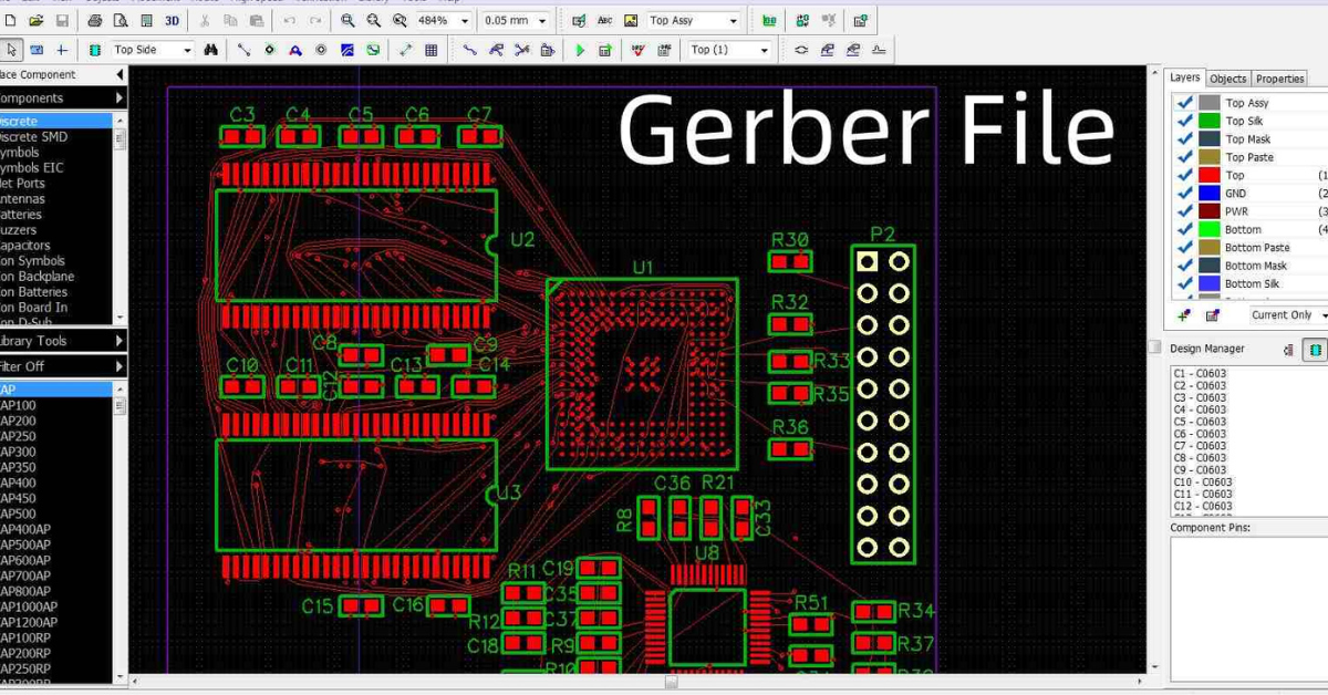
Gerber file viewers are software tools that render Gerber files into visual representations, allowing engineers to inspect each layer of a PCB design. Unlike PCB design software, which focuses on creating and editing layouts, Gerber viewers are lightweight tools designed for verification. They enable you to check for errors, measure distances, and ensure compliance with manufacturing requirements.
Key functions of Gerber viewers include:
-
Layer Visualization: Display individual or overlaid PCB layers to check alignment and completeness.
-
Measurement Tools: Verify trace widths, spacing, and hole sizes against design rules (e.g., ensuring a 0.2 mm clearance between traces for 100 V isolation).
-
Design for Manufacturing (DFM) Checks: Identify issues like insufficient solder mask clearance or overlapping drill holes.
-
File Comparison: Compare different revisions of Gerber files to detect unintended changes.
By using a Gerber viewer, you can catch errors that might otherwise lead to scrapped boards or costly rework. For instance, a common mistake is exporting a Gerber file with an incorrect aperture list, which can distort pad sizes and affect solderability.
Top Gerber Viewer Tools for Engineers
Several Gerber viewer tools are available, each with unique features suited for different needs. Here are some of the most popular options, based on their functionality and ease of use:
1. Gerbv
Gerbv, an open-source viewer part of the gEDA project, is widely used for its simplicity and compatibility with RS-274X and X2 formats. It supports Linux, Windows, and UNIX, making it versatile for engineers working across platforms. Key features include layer overlay, measurement tools, and the ability to export rendered images for documentation. Gerbv is ideal for hobbyists or small teams due to its free cost and lightweight design.
2. Altium 365 Viewer
Altium 365 offers a cloud-based Gerber viewer that integrates seamlessly with Altium Designer. It supports RS-274X, X2, and ODB++ formats, and its comparison feature allows side-by-side analysis of file revisions. The viewer's real-time DFM checks can flag issues like insufficient annular ring sizes (e.g., <0.15 mm), which could cause drilling errors. This tool is best for professional teams needing advanced collaboration features.
3. ViewMate
Pentalogix ViewMate is a free Windows-based viewer with robust DFM analysis capabilities. It supports Gerber, ODB++, and Excellon formats, and its Smart DFM feature checks for manufacturability issues, such as acid traps or incomplete solder masks. ViewMate's deluxe version offers additional tools like netlist comparison, making it suitable for complex designs.
4. EasyEDA
EasyEDA's online Gerber viewer combines viewing with basic PCB editing capabilities. It supports layer stacking visualization and zoom functions, allowing engineers to check fine details like 0.1 mm trace widths. EasyEDA is a great choice for engineers who want an all-in-one platform for design and verification.
Each tool has its strengths, so choose one based on your project's complexity and budget. For example, Gerbv is sufficient for simple two-layer boards, while Altium 365 is better for multilayer HDI designs.
How to Use a Gerber Viewer Effectively
To maximize the benefits of a Gerber viewer, follow these steps to ensure your files are error-free before fabrication:
Step 1: Validate Layer Alignment
Load all Gerber files into the viewer and check that layers align correctly. Misaligned layers can cause short circuits or open connections. For example, ensure the top copper layer aligns with the top solder mask to avoid exposed traces, which could lead to corrosion.
Step 2: Verify Design Rules
Use the viewer's measurement tools to confirm that trace widths, clearances, and hole sizes meet your design rules. For high-speed designs, verify that differential pair spacing (e.g., 0.15 mm for 10 Gbps signals) matches the required impedance (typically 100 ohms ±10%).
Step 3: Check Drill Files
Inspect the drill file (usually in Excellon format) to ensure hole sizes and locations are correct. A common error is mismatched plated and non-plated holes, which can affect via functionality. For instance, a 0.3 mm drill hole with a 0.5 mm pad requires a minimum annular ring of 0.1 mm to ensure reliable plating.
Step 4: Perform DFM Checks
Run DFM checks to identify manufacturability issues, such as insufficient solder mask clearance (e.g., <0.05 mm), which can cause solder bridging. Some viewers, like ViewMate, automate these checks, highlighting potential problems in red.
Step 5: Compare Revisions
If you've updated your design, use the viewer's comparison feature to ensure only intended changes were made. Unintended modifications, like a shifted silkscreen logo, can cause confusion during assembly.
Step 6: Export and Share
Once verified, export screenshots or reports from the viewer to share with your manufacturer or team. This ensures everyone is on the same page regarding the design intent.
By following these steps, you can catch errors early, reducing the risk of defective boards. For example, spotting a 0.2 mm solder mask misalignment before production can prevent a batch of boards from failing at 100 MHz due to signal crosstalk.
Common Gerber File Errors and How to Spot Them
Even experienced engineers can make mistakes when generating Gerber files. Here are some common errors and how to identify them using a Gerber viewer:
-
Incorrect Aperture Lists: An incorrect aperture list can distort pad or trace shapes. Check the viewer's aperture report to ensure all shapes match your design.
-
Layer Mislabeling: Files labeled as 'top copper' but containing bottom copper data can confuse manufacturers. Verify layer names and contents in the viewer.
-
Missing Drill Files: Without a drill file, holes won't be drilled. Confirm that the drill file is included and matches the Gerber data.
-
Solder Mask Misalignment: A misaligned solder mask can expose traces or cover pads. Overlay the solder mask and copper layers to check for alignment.
-
Zero-Width Traces: Traces exported with zero width won't appear on the board. Use the viewer's zoom function to inspect trace continuity.
Spotting these errors before fabrication can save significant time and cost. For instance, a missing drill file could delay production by days, while a solder mask misalignment might require a complete redesign.
Best Practices for Generating Gerber Files
While Gerber viewers help catch errors, generating accurate files from the start is equally important. Follow these best practices:
-
Run Design Rule Checks (DRC): Before exporting, run DRC in your PCB design software to catch issues like insufficient spacing (e.g., <0.15 mm for 50 V isolation).
-
Use Standard Formats: Export in RS-274X or X2 format for maximum compatibility. Avoid obsolete formats like RS-274D.
-
Include All Layers: Ensure all necessary layers (copper, solder mask, silkscreen, drill) are exported. For a four-layer board, this typically means at least seven files.
-
Add Polarity Marks: Include a small polarity mark (e.g., a 0.5 mm hole) to aid layer alignment during fabrication.
-
Communicate with Your Manufacturer: Confirm file requirements, such as preferred extensions (.gbr, .top, .bot) or compression formats (e.g., ZIP).
By combining these practices with thorough Gerber viewer inspections, you can minimize errors and streamline the fabrication process.
How ALLPCB Supports Error-Free PCB Fabrication
At ALLPCB, we understand the importance of precision in PCB fabrication. Our advanced manufacturing facilities and quick-turn prototyping services help engineers bring their designs to life with confidence. By using our online Gerber viewer, you can upload and inspect your files directly on our platform, ensuring they meet our stringent DFM standards. Our global logistics network ensures fast delivery, with prototypes shipped in as little as 24 hours for standard two-layer boards. Whether you're working on a high-speed design or a compact IoT device, ALLPCB's expertise and tools, including real-time DFM feedback, help you achieve error-free fabrication every time.
Conclusion
Gerber file viewers are indispensable tools for ensuring error-free PCB fabrication. By allowing engineers to visualize, measure, and verify their designs, these tools catch issues that could otherwise lead to defective boards or costly delays. Whether you're using a free tool like Gerbv or a professional platform like Altium 365, the key is to follow a systematic verification process, from checking layer alignment to running DFM checks. Combined with best practices for generating Gerber files, these tools empower you to deliver high-quality PCBs that meet your design specifications.
As you prepare your next PCB design, take the time to leverage a Gerber viewer to inspect your files thoroughly. The small investment in verification can save you from the headaches of manufacturing errors, ensuring your boards perform reliably in the field. At ALLPCB, we're here to support you with tools and services that make precision fabrication seamless and efficient.