Microelectronics assembly is a critical cornerstone in the world of modern electronics, enabling the creation of compact, high-performance devices that power everything from smartphones to medical equipment. If you're looking for a comprehensive resource on the microelectronics assembly process flow, the microelectronics assembly challenges, or the latest microelectronics assembly innovations, you've come to the right place. This guide dives deep into the intricate world of microelectronics assembly, offering practical insights into processes, hurdles, and cutting-edge advancements. Whether you're an engineer, a designer, or a manufacturer, this blog will equip you with the knowledge to navigate this complex field.
Let’s explore the detailed workflows, uncover the common obstacles, and highlight the innovative techniques shaping the future of microelectronics assembly. From advanced microelectronics assembly techniques to microelectronics assembly best practices, we’ve got it all covered in this ultimate guide.
What Is Microelectronics Assembly?
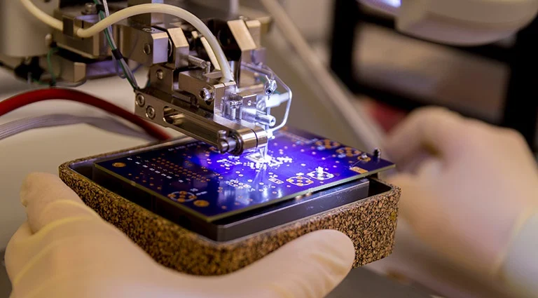
Microelectronics assembly refers to the process of constructing tiny electronic components and circuits, often at a microscopic scale, to create functional devices. These components, such as integrated circuits (ICs), microprocessors, and sensors, are assembled into packages or systems that can be integrated into larger electronic products. The precision required in this field is immense, as even the smallest error can lead to device failure.
The importance of microelectronics assembly lies in its role in miniaturization and performance enhancement. As devices become smaller and more powerful, the demand for precise assembly techniques grows. This guide will walk you through every aspect of the process, from start to finish, while addressing key pain points and showcasing modern solutions.
Microelectronics Assembly Process Flow: A Step-by-Step Breakdown
Understanding the microelectronics assembly process flow is essential for anyone involved in electronics manufacturing. This process involves multiple stages, each requiring precision and specialized tools. Below is a detailed look at the typical workflow:
1. Wafer Fabrication
The journey begins with wafer fabrication, where thin slices of semiconductor material, often silicon, are processed to create the base for microelectronic components. This stage involves photolithography, etching, and doping to form intricate circuit patterns. The wafers are typically 300 mm in diameter and must be handled in ultra-clean environments to avoid contamination.
2. Die Preparation and Dicing
Once the wafer is complete, it is cut into individual chips or "dies" using a high-precision dicing saw. Each die contains a complete circuit, and this step requires extreme accuracy to prevent damage. The dies are then cleaned and inspected for defects.
3. Die Bonding
In this stage, the individual dies are attached to a substrate or package using adhesive materials or soldering. The bonding process must ensure a strong mechanical connection and excellent thermal conductivity. For high-performance devices, eutectic bonding with gold-tin alloys is often used, providing a reliable joint at temperatures around 280°C.
4. Wire Bonding or Flip-Chip Bonding
Next, electrical connections are made between the die and the package. Wire bonding uses thin gold or aluminum wires (about 25 micrometers in diameter) to connect the die to external leads. Alternatively, flip-chip bonding places the die face-down, connecting it directly to the substrate using tiny solder bumps. This method reduces signal delay, often achieving latency improvements of up to 50% compared to traditional wire bonding.
5. Encapsulation
To protect the delicate components from environmental factors like moisture and dust, the assembly is encapsulated using materials like epoxy resin. This step also enhances mechanical stability. The encapsulation process must be carefully controlled to avoid introducing stress that could crack the die.
6. Testing and Quality Assurance
Finally, the assembled microelectronics undergo rigorous testing to ensure functionality. This includes electrical testing for parameters like impedance (often in the range of 50 ohms for high-frequency applications) and signal integrity. Only units that pass these tests move on to final packaging and shipping.

Microelectronics Assembly Challenges: Common Obstacles and Solutions
While the assembly process is highly sophisticated, it comes with significant microelectronics assembly challenges. Addressing these hurdles is crucial for maintaining quality and efficiency in production. Let’s explore some of the most common issues and how they can be mitigated.
1. Miniaturization and Precision
As devices shrink, the components become increasingly tiny, often measuring less than 100 micrometers. Assembling such small parts requires ultra-precise equipment and cleanroom environments with particle counts as low as 10 particles per cubic meter. Even a slight misalignment can lead to connection failures or signal loss.
Solution: Invest in automated assembly systems with vision-guided robotics capable of handling components with sub-micron accuracy. Regular calibration of equipment is also vital to maintain precision.
2. Thermal Management
Microelectronics generate significant heat in a confined space, with power densities sometimes exceeding 100 W/cm2. Poor thermal management can cause overheating, reducing device lifespan or causing immediate failure.
Solution: Use advanced materials like thermal interface materials (TIMs) with high conductivity (up to 5 W/m·K) to dissipate heat effectively. Additionally, integrating microchannel cooling systems into the design can enhance heat removal.
3. Contamination and Defects
Contamination from dust, moisture, or residues during assembly can compromise performance. A single particle on a die can short-circuit connections, leading to failure rates as high as 20% in poorly controlled environments.
Solution: Maintain strict cleanroom standards and implement real-time monitoring systems to detect contaminants. Automated cleaning processes before encapsulation can also reduce defect rates.
4. Cost and Scalability
The high cost of equipment and materials, combined with the need for skilled labor, makes microelectronics assembly expensive. Scaling production while maintaining quality adds another layer of complexity.
Solution: Adopt modular assembly lines that can be scaled based on demand. Leveraging automation reduces labor costs and improves consistency, making large-scale production more feasible.
Microelectronics Assembly Innovations: Shaping the Future
The field of microelectronics is evolving rapidly, with microelectronics assembly innovations driving improvements in efficiency, performance, and scalability. Here are some of the most exciting advancements transforming the industry.
1. 3D Packaging and Stacking
Traditional 2D layouts are giving way to 3D packaging, where multiple dies are stacked vertically. This approach reduces the footprint and shortens interconnect lengths, improving signal speeds by up to 30%. Through-silicon vias (TSVs) enable vertical connections with minimal latency.
2. Advanced Bonding Techniques
Innovations like hybrid bonding combine direct copper-to-copper connections with dielectric bonding, eliminating the need for solder bumps. This technique supports finer pitch connections (down to 10 micrometers) and enhances reliability in high-density applications.
3. Automation and AI Integration
Automation, powered by artificial intelligence, is revolutionizing assembly lines. AI algorithms can predict equipment failures, optimize process parameters, and detect defects with over 95% accuracy, significantly reducing downtime and waste.
4. Sustainable Materials
With environmental concerns on the rise, the industry is shifting toward eco-friendly materials for encapsulation and substrates. Biodegradable polymers and lead-free solders are gaining traction, reducing the ecological footprint of microelectronics manufacturing.
Advanced Microelectronics Assembly Techniques for Optimal Results
Implementing advanced microelectronics assembly techniques can elevate the quality and performance of your products. Below are some cutting-edge methods to consider:
1. Wafer-Level Packaging (WLP)
WLP involves packaging the die directly on the wafer before dicing, reducing handling steps and costs. This technique is ideal for high-volume production and supports ultra-thin devices with thicknesses below 100 micrometers.
2. Microfluidic Cooling Integration
For high-power applications, embedding microfluidic channels into the substrate allows for efficient cooling. These channels can reduce operating temperatures by up to 20°C, extending device lifespan.
3. Laser-Assisted Bonding
Laser bonding offers precise control over heat application, minimizing thermal stress on delicate components. This method achieves bond strengths comparable to traditional soldering but with faster processing times, often under 5 seconds per connection.
By adopting these techniques, manufacturers can achieve higher yields and better performance, staying ahead in a competitive market.
Microelectronics Assembly Best Practices for Success
To ensure consistent quality and efficiency, following microelectronics assembly best practices is essential. Here are actionable tips to optimize your assembly process:
- Maintain Cleanroom Standards: Adhere to ISO Class 5 or better cleanroom standards to minimize contamination. Regularly monitor particle levels and humidity (ideally 40-50%) to protect sensitive components.
- Invest in Training: Equip your team with the latest skills in handling micro-scale components and operating advanced machinery. Continuous learning ensures adaptability to new technologies.
- Use Real-Time Monitoring: Implement sensors and software to track process variables like temperature and alignment in real time. This helps catch issues early, reducing defect rates by up to 15%.
- Prioritize Material Selection: Choose substrates and adhesives with matching thermal expansion coefficients to prevent cracking during temperature cycles. For instance, using materials with a coefficient of thermal expansion (CTE) of 3-5 ppm/°C can minimize stress.
- Conduct Thorough Testing: Test assemblies under real-world conditions, including thermal cycling from -40°C to 85°C, to ensure reliability before market release.
Conclusion: Navigating the Future of Microelectronics Assembly
Microelectronics assembly is a dynamic and challenging field that sits at the heart of technological advancement. By understanding the microelectronics assembly process flow, tackling microelectronics assembly challenges, and embracing microelectronics assembly innovations, manufacturers can produce cutting-edge devices that meet the demands of today’s market. Leveraging advanced microelectronics assembly techniques and adhering to microelectronics assembly best practices ensures high-quality outcomes and positions you as a leader in the industry.
At ALLPCB, we are committed to supporting your journey in microelectronics assembly with top-tier solutions and expertise. Whether you’re optimizing an existing process or exploring new technologies, this guide serves as your roadmap to success. Keep pushing the boundaries of what’s possible, and let precision drive your innovation.
 ALLPCB


