 ALLPCB


Are you struggling with component placement on a single-sided PCB? Proper placement is key to ensuring functionality, manufacturability, and reliability in your design. In this comprehensive guide, we’ll walk you through the best practices for single-sided PCB component placement, including tips for SMD and through-hole components, and strategies for optimal layout. Whether you're a beginner or a seasoned engineer, this guide will help you master the art of component placement for efficient and high-performing PCB assembly.
Why Component Placement Matters in Single-Sided PCB Assembly
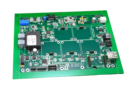
Single-sided PCBs are widely used in simple electronics due to their cost-effectiveness and ease of manufacturing. However, with components placed on only one side of the board and limited space for traces, effective component placement becomes critical. Poor placement can lead to signal interference, overheating, or assembly issues, ultimately affecting the performance of your device.
By focusing on strategic single-sided PCB component placement, you can minimize trace lengths, reduce noise, and ensure a smooth assembly process. Let’s dive into the core principles and techniques that will help you achieve a well-organized layout.
Key Challenges of Single-Sided PCB Component Placement
Before we explore the best practices, it’s important to understand the unique challenges of working with single-sided PCBs:
- Limited Space: With only one side available for components and traces, overcrowding can lead to routing difficulties.
- Signal Integrity Issues: Longer traces due to poor placement can introduce noise or delay in high-speed signals, often exceeding acceptable thresholds like 50 ohms impedance mismatch.
- Thermal Management: Components generating heat, such as power regulators, need proper spacing to avoid overheating adjacent parts.
- Manufacturing Constraints: Incorrect placement can complicate soldering processes, especially for automated assembly lines.
Understanding these challenges sets the foundation for making informed decisions during the design phase. Let’s now look at actionable strategies for optimal component placement on single-sided PCBs.
General Best Practices for Single-Sided PCB Component Placement
Following a set of proven guidelines can significantly improve the performance and manufacturability of your single-sided PCB. Here are the core principles to keep in mind:
1. Plan Your Layout Before Placement
Start by creating a rough sketch or digital layout of your PCB. Group components based on their function, such as power supply, analog, and digital sections. This helps reduce interference and keeps traces short. For instance, placing a microcontroller close to its supporting capacitors can minimize noise on a 3.3V line.
2. Prioritize Critical Components
Place high-priority components like connectors, power ICs, and microcontrollers first. These often dictate the placement of other parts. For example, position connectors near the board edges for easy access, and place power ICs where heat dissipation is feasible.
3. Minimize Trace Lengths
Shorter traces reduce signal loss and electromagnetic interference (EMI). Aim to keep critical signal traces under 10-15 mm if possible, especially for high-speed signals operating at 100 MHz or above. Arrange components to allow direct, straight paths for traces on the single-sided board.
4. Maintain Proper Spacing
Ensure adequate spacing between components to avoid soldering issues and thermal overlap. A general rule is to maintain at least 0.5 mm between SMD components and 1-2 mm for through-hole parts, depending on the assembly process.
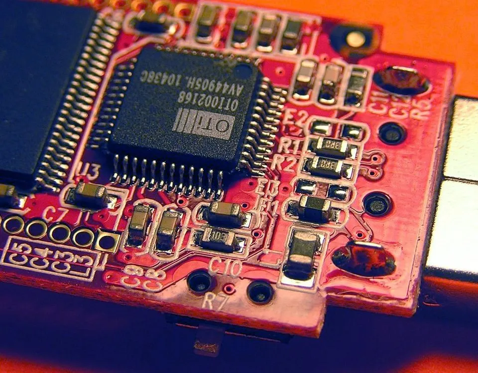
SMD Component Placement on Single-Sided PCBs
Surface-mount device (SMD) components are popular in modern PCB designs due to their small size and compatibility with automated assembly. However, SMD component placement on single-sided PCBs requires precision to avoid issues during soldering and operation. Here are some tips tailored for SMDs:
1. Orient SMD Components for Easy Assembly
Align SMD components in the same direction whenever possible. For example, orient all resistors and capacitors horizontally or vertically to streamline the pick-and-place process during manufacturing. This also reduces the risk of tombstoning, where one end of the component lifts during soldering.
2. Avoid Overcrowding SMD Pads
Ensure there’s at least 0.3-0.5 mm clearance between SMD pads to prevent solder bridges. Overcrowding can lead to short circuits, especially with fine-pitch components like 0402 or 0201 packages.
3. Place Decoupling Capacitors Close to ICs
For SMD capacitors used in decoupling, position them as close as possible to the power pins of ICs. Ideally, keep the distance under 5 mm to reduce inductance and maintain a stable voltage supply, such as 5V or 3.3V, depending on the circuit.
4. Consider Reflow Soldering Constraints
During reflow soldering, heat distribution can vary across the board. Place larger SMD components away from smaller ones to avoid uneven heating, which can cause defects like cold solder joints.
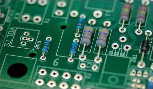
Through-Hole Component Placement on Single-Sided PCBs
Through-hole components are often used in single-sided PCBs for their durability and ease of manual assembly. However, their placement requires careful planning to ensure a robust design. Here’s how to approach through-hole component placement on single-sided PCBs:
1. Secure Mechanical Stability
Place larger through-hole components, such as connectors or electrolytic capacitors, in areas where they can be firmly secured to the board. This prevents mechanical stress during handling or operation. For example, a large 1000 μF capacitor should be placed where it won’t interfere with other components if the board is tilted.
2. Optimize for Manual Soldering
Arrange through-hole components with enough space around their leads for easy soldering. A minimum clearance of 1.5-2 mm between through-hole pads is ideal for hand soldering, ensuring no overlap during the process.
3. Group by Height
Position taller through-hole components away from shorter ones to avoid shadowing during assembly or testing. For instance, keep a 10 mm tall capacitor away from low-profile resistors to maintain accessibility.
4. Align for Wave Soldering
If wave soldering is used, orient through-hole components in the same direction and place them to minimize shadowing effects. This ensures even solder flow across all leads, reducing the risk of defects.
Strategies for Optimal Component Placement on Single-Sided PCBs
Achieving optimal component placement on a single-sided PCB requires balancing functionality, manufacturability, and performance. Here are advanced strategies to refine your layout:
1. Separate Analog and Digital Sections
To prevent noise interference, keep analog and digital components in distinct areas of the board. For example, place an analog sensor at least 10-15 mm away from a digital microcontroller to avoid crosstalk on sensitive signals like a 1 mV analog output.
2. Manage Thermal Hotspots
Identify components that generate significant heat, such as voltage regulators or power transistors, and place them near the board’s edges or in areas with good airflow. Ensure a clearance of at least 5-10 mm around these components to prevent thermal damage to nearby parts.
3. Use a Ground Plane Effectively
Even on a single-sided PCB, a partial ground plane can improve signal integrity. Place components strategically to connect to the ground plane with short traces, reducing EMI. For instance, grounding pins of an IC should connect to the plane within 5 mm for optimal performance.
4. Test Accessibility
Ensure test points and critical components are accessible for debugging. Place test pads near the edges or in open areas, avoiding overlap with densely packed components. This simplifies troubleshooting without requiring disassembly.
Common Mistakes to Avoid in Single-Sided PCB Component Placement
Even experienced designers can make errors that impact the quality of a single-sided PCB. Here are some pitfalls to watch out for:
- Ignoring Component Orientation: Misaligned components can complicate assembly and lead to errors like incorrect polarity in capacitors or diodes.
- Overcrowding the Board: Packing components too tightly can cause soldering defects and make rework difficult.
- Neglecting Thermal Design: Failing to account for heat dissipation can lead to component failure, especially in power-intensive circuits.
- Poor Trace Planning: Not considering trace routing during placement can result in long, convoluted paths that degrade signal quality.
Tools and Software for Single-Sided PCB Layout Design
Using the right tools can simplify the process of component placement. Many design software platforms offer features like auto-placement and design rule checks (DRC) to help optimize your layout. Look for software that supports single-sided PCB designs and provides real-time feedback on spacing and trace lengths. These tools often include libraries with standard component footprints, ensuring accurate placement for both SMD and through-hole parts.
Run simulations to verify signal integrity and thermal performance before finalizing your design. This step can identify potential issues, such as a trace impedance mismatch exceeding 10 ohms, allowing you to adjust placement accordingly.
Conclusion: Mastering Single-Sided PCB Component Placement
Effective component placement is the cornerstone of a successful single-sided PCB assembly. By following the best practices outlined in this guide, you can overcome the challenges of limited space and ensure your design is both functional and manufacturable. Whether you’re working with SMD or through-hole components, strategic placement minimizes signal issues, improves thermal management, and streamlines the assembly process.
Start with a clear plan, prioritize critical components, and always consider the manufacturing constraints of single-sided PCBs. With these tips for single-sided PCB component placement, SMD component placement on single-sided PCBs, through-hole component placement on single-sided PCBs, and optimal component placement strategies, you’re well-equipped to create high-quality designs that meet your project’s needs.
Take the time to refine your layout, test your design, and iterate as needed. A well-thought-out component placement not only enhances performance but also saves time and cost during production. Let’s build better PCBs together!


